Microfabricated inductors with through-wafer vias

a technology of through-wafer vias and microfabricated inductors, which is applied in the direction of magnets, magnetic bodies, and semiconductor/solid-state device details, etc., can solve the problems of reducing the performance of rf systems at high frequencies, limiting or hampering the ability to reduce the size of rf systems, and requiring a large amount of physical space for conventional inductors with air centers

Inactive Publication Date: 2010-09-09
TELEDYNE SCI & IMAGING
View PDF5 Cites 35 Cited by
  • Summary
  • Abstract
  • Description
  • Claims
  • Application Information

AI Technical Summary

Problems solved by technology

However, conventional inductors with an air center require a large amount of physical space and may also have a relatively low Q factor.
This can place a lim...

Method used


Image

  • Microfabricated inductors with through-wafer vias
  • Microfabricated inductors with through-wafer vias
  • Microfabricated inductors with through-wafer vias

Examples


Embodiment Construction

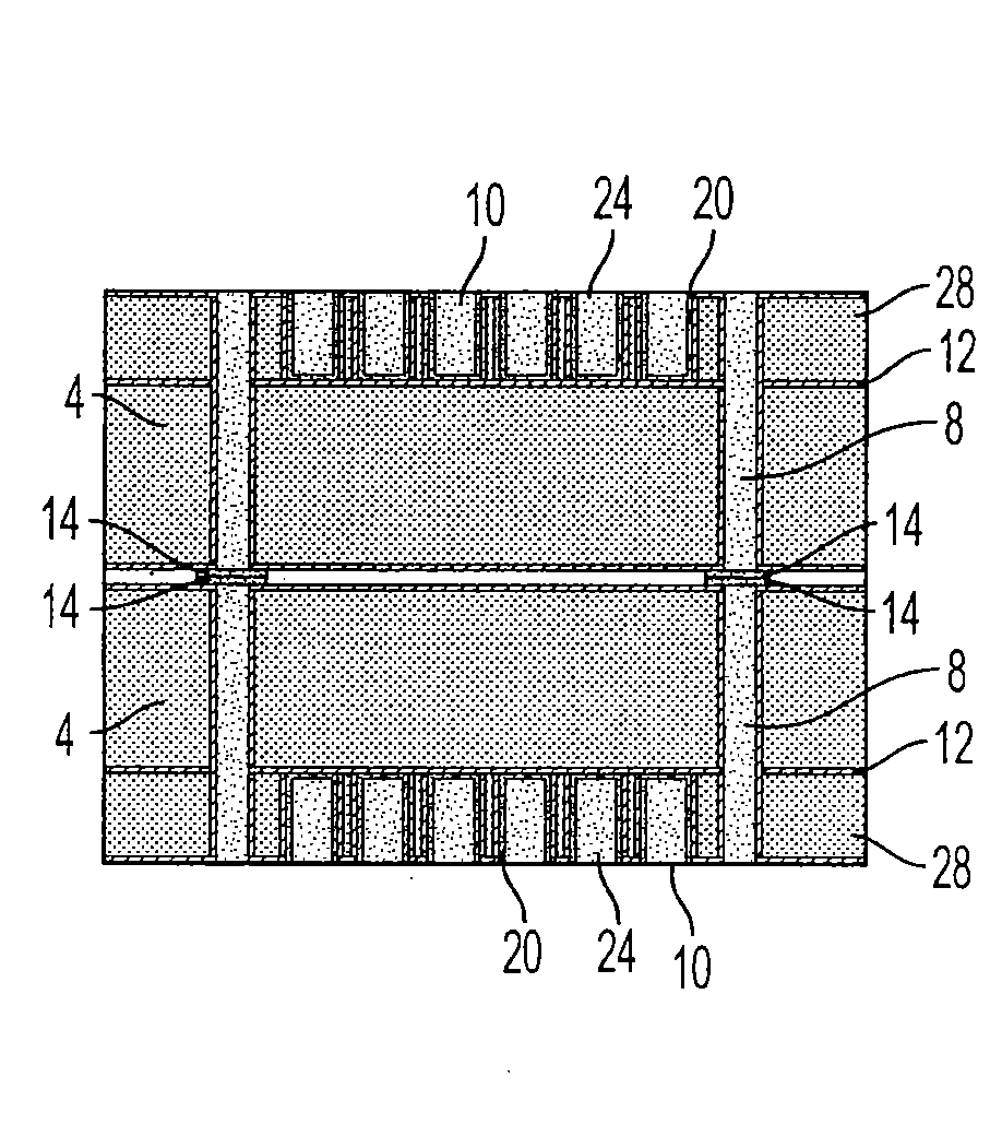
[0047]Methods and systems that implement the embodiments of the various features of the present invention will now be described with reference to the drawings. The drawings and the associated descriptions are provided to illustrate embodiments of the present invention and not to limit the scope of the present invention. Reference in the specification to “one embodiment” or “an embodiment” is intended to indicate that a particular feature, structure, or characteristic described in connection with the embodiment is included in at least an embodiment of the present invention. The appearances of the phrase “in one embodiment” or “an embodiment” in various places in the specification are not necessarily all referring to the same embodiment. Throughout the drawings, reference numbers are re-used to indicate correspondence between referenced elements.

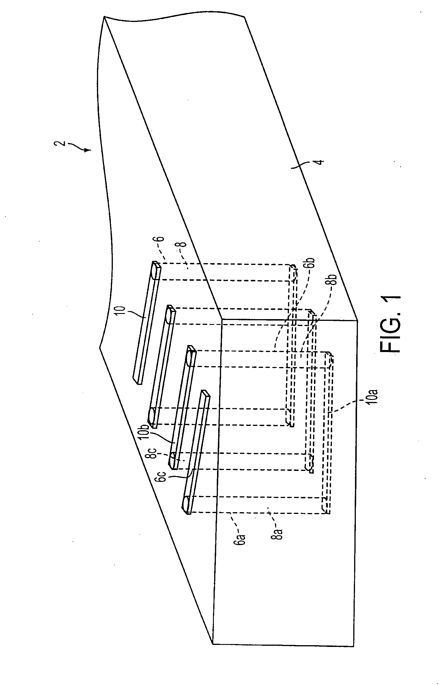
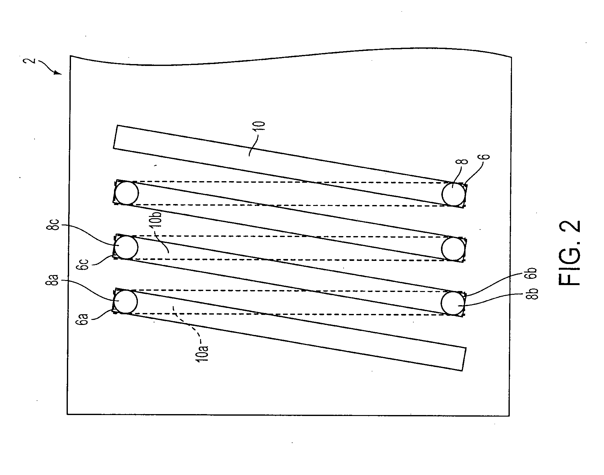
[0048]FIG. 1 is a perspective view of an embodiment of the present invention while FIG. 2 is a top view of an embodiment of the present inven...


PUM

PropertyMeasurementUnit
Electrical resistanceaaaaaaaaaa
Densityaaaaaaaaaa
Depthaaaaaaaaaa

Abstract

The present invention relates to microfabricated inductors with through-wafer vias. In one embodiment, the present invention is an inductor including a first wafer, a first plurality of metal fillings located within the first wafer, and a first plurality of metal conductors connecting the first plurality of metal fillings together to form a first spiral with a first plurality of windings. In another embodiment, the present invention is a method for producing an inductor including the steps of forming a first plurality of vias in a first substrate, filling the first plurality of vias in the first substrate with a first plurality of metal fillings, forming a first plurality of metal conductors, and connecting pairs of the first plurality of metal fillings together using the first plurality of metal conductors to form a spiral.

Description

BACKGROUND[0001]1. Field[0002]The present invention relates to microfabricated inductors with through-wafer vias.[0003]2. Related Art[0004]RF systems often use inductors. However, conventional inductors with an air center require a large amount of physical space and may also have a relatively low Q factor. This can place a limit or hamper the ability of reducing the size of RF systems. Furthermore, the relatively low Q factor can reduce the performance of RF systems at high frequencies.[0005]Thus, there is a need for inductors which occupy a reduced amount of space and possess an improved Q factor.SUMMARY[0006]In one embodiment, the present invention is an inductor including a first wafer, a first plurality of metal fillings located within the first wafer, and a first plurality of metal conductors connecting the first plurality of metal fillings together to form a first spiral with a first plurality of windings.[0007]In another embodiment, the present invention is an inductor includ...

Claims


Application Information

Patent Timeline
IPC IPC(8): H01F5/00H01F7/06
CPCH01F17/0013H01F2017/0086Y10T29/49165Y10T29/49073Y10T29/4902H01F17/03H01L21/76898H01L23/481H01L23/5227H01L21/2885
Inventor PAPAVASILIOU, ALEXANDROSDENATALE, JEFFREY F.STUPAR, PHILIP A.BORWICK, III, ROBERT L.
Owner TELEDYNE SCI & IMAGING
Why Eureka
Try Eureka