[0013]Accordingly, preferred embodiments of the present invention provide a laminated ceramic electronic component including a single ceramic element body including a plurality of effective sections which constitute circuit elements such as capacitor units, for example. In the laminated ceramic electronic component, bumps generated in the ceramic element body are minimized in size. Furthermore, the laminated ceramic electronic component is fabricated without the use of a high-accuracy printing technique but instead with comparatively simple steps, and therefore, is low in cost.
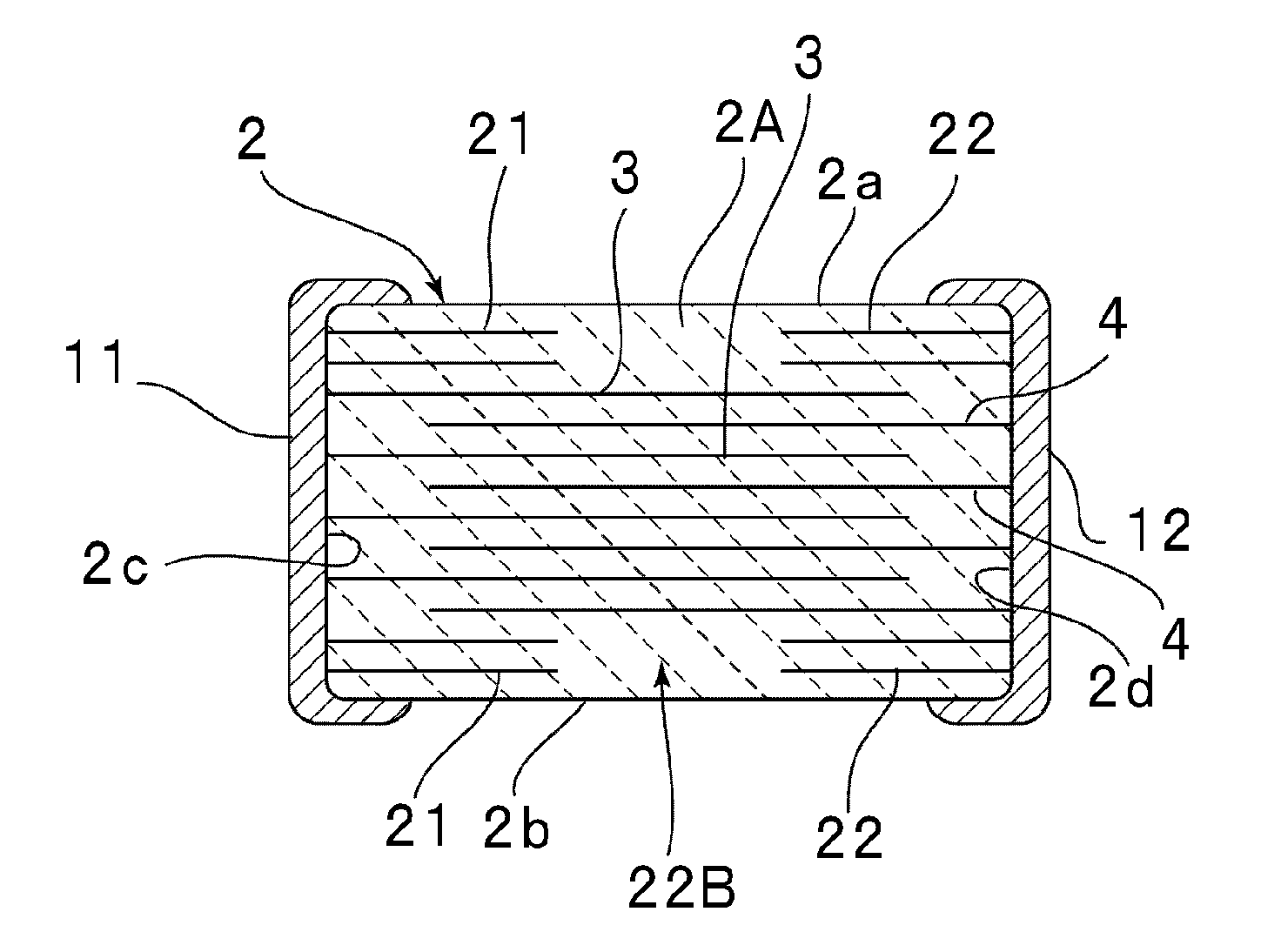
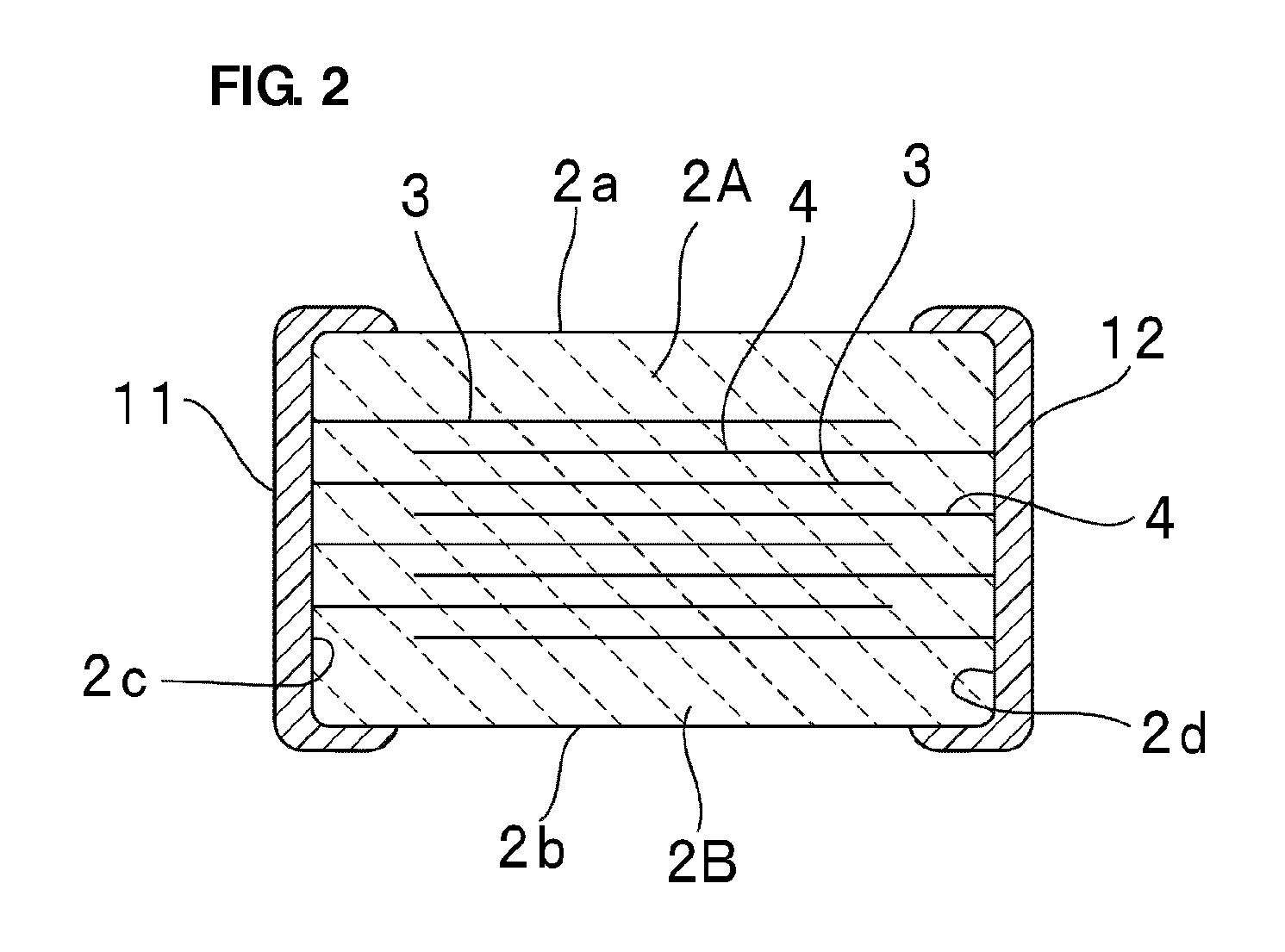
[0016]The first effective section may include first internal conductors electrically connected to the first external terminal
electrode and second internal conductors electrically connected to the second external terminal
electrode, the first and second internal conductors being laminated on one another through ceramic
layers. The second effective section may include third internal conductors electrically connected to the third external terminal
electrode and fourth internal conductors electrically connected to the fourth external terminal electrode, the third and fourth internal conductors being laminated on one another through ceramic
layers. In this case, each of the effective units can be configured as a laminated circuit element such as a laminated capacitor unit, a laminated
thermistor unit, a laminated
inductor unit, or a laminated
piezoelectric resonance unit, and
miniaturization of electronic component can be enhanced.
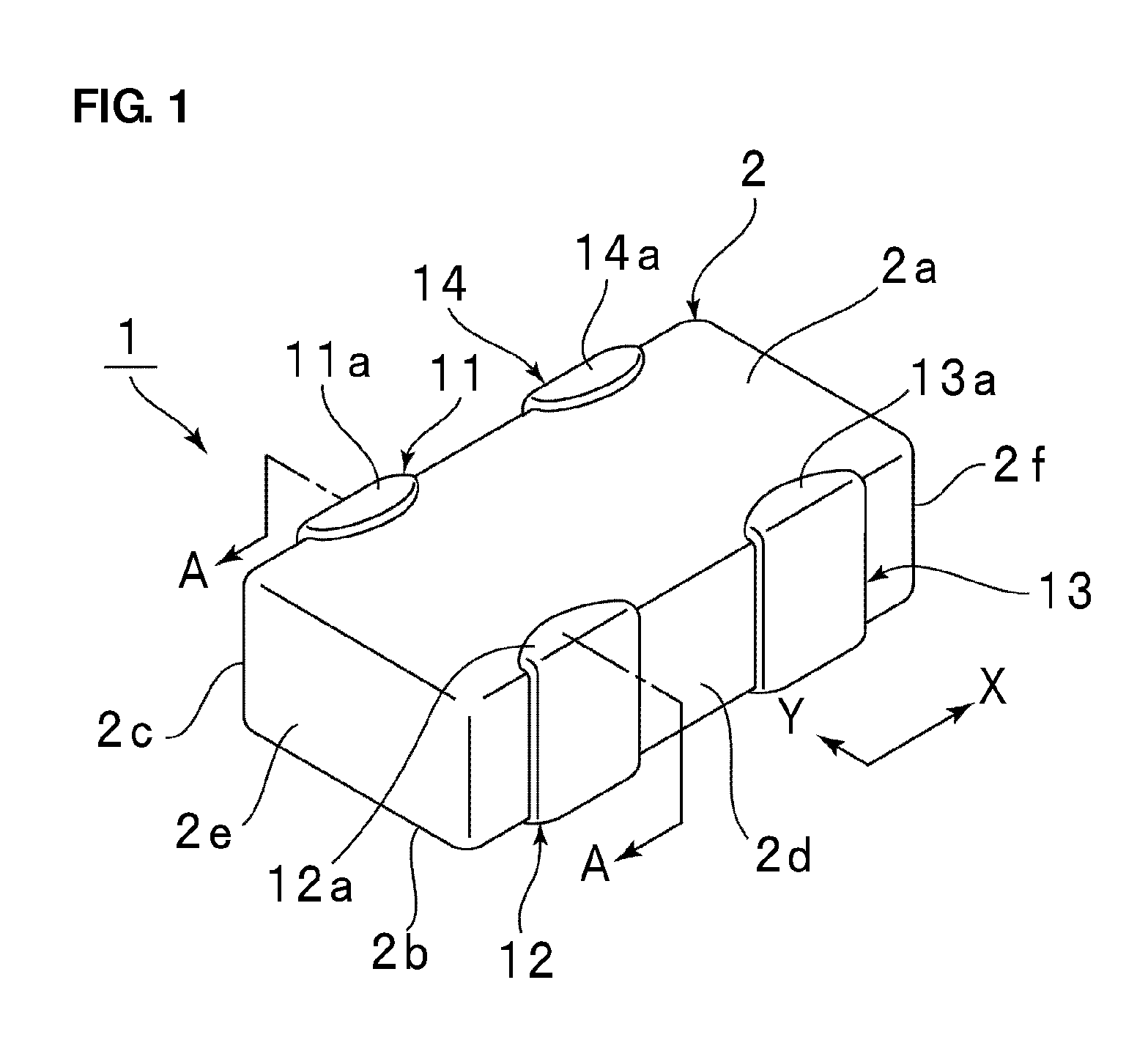
[0017]The first and third external terminal electrodes may be provided on the first side surface, the second and fourth external electrodes may be provided on the second side surface, the first and second external terminal electrodes may face each other through the ceramic element body, and the third and fourth external electrodes may face each other through the ceramic element body. In this case, since the first side surface in which the first and third external terminal electrodes are arranged faces the second side surface in which the second and fourth external terminal electrodes which are connected to a potential different from a potential connected to the first and third external terminal electrodes are arranged, an operation of electrically connecting the laminated ceramic electronic component to an external device can be easily performed.
[0018]The first to fourth external terminal electrodes may have external terminal-electrode extending portions on the first and second main surfaces, and distances among centers of the external terminal-electrode extending portions of the first to fourth terminal electrodes adjacent to one another may be substantially equal to one another in each of the first and second main surfaces. In this case, direction determination of the laminated ceramic electronic component can be easily performed using the floating internal conductors as makers.
[0020]The laminated ceramic electronic component may further include a dummy internal conductor which is electrically connected to one of the first to fourth external terminal electrodes in at least one of the first and second external layer sections. In this case, since the first and second internal conductors are exposed to the surfaces of the ceramic element body and electrically connected to the external terminal electrodes, joint strength of the external terminal electrodes can be enhanced. Furthermore, in a case where the external terminal electrodes are formed by a plating method, the number of starting points for plating is increased. Accordingly, the external terminal electrodes can be reliably and easily formed by the plating method.
[0026]Furthermore, the floating internal conductor can be easily formed by forming a
dielectric film by printing
conductive paste on a ceramic green sheet to be an external layer section or by a thin-film formation method such as plating or
evaporation when the laminated ceramic electronic component 1 is fabricated. In addition, a printing method which requires high accuracy is not necessary. Accordingly, complicated fabrication steps of the laminated ceramic electronic component can be prevented and cost of the laminated ceramic electronic component can be reduced.

