Method for Laser Singulation of Chip Scale Packages on Glass Substrates

a technology of chip scale and glass substrate, applied in the field of electronic devices singulation, can solve the problems of difficult singulation of compound electronic devices, and achieve the effects of avoiding cracks or chips, reducing the size of streets, and acceptable cutting speeds

Inactive Publication Date: 2010-09-30
ELECTRO SCI IND INC
View PDF72 Cites 139 Cited by
  • Summary
  • Abstract
  • Description
  • Claims
  • Application Information

AI Technical Summary

Benefits of technology

[0013]One object of the instant invention is to provide a method for singulation of compound electronic devices. Another object of the instant invention is to provide a method for singulation of compound electronic devices that avoids creating cracks or chips while maintaining acceptable cutting speeds. A further object of the instant invention is to provide a method for singulation of compound electronic devices that minimizes the size of streets. Compound electronic devices are particularly difficult to singulate due to their construction with two or more substrates requiring simultaneous separation to perform singulation. In particular, image sensor devices typically contain both active electronic device substrates such as silicon and transparent protective substrates made of glass or glass-like material, typically with differing thicknesses. One embodiment of the invention disclosed herein uses different separation techniques for different layers in the compound semiconductor device. In particular, at least one substrate is diced or laser machined to form a through-cut kerf while at least one other layer is scribed and subsequently mechanically cleaved.
[0017]FIGS. 8a and b illustrate the effect of directing a laser beam through the cut made in the first substrate. The laser beam is measured using a setup like FIG. 6c, where the laser beam 80 passes through a cut 98 in a first substrate 82. The laser beam profile is measured as if it were impinging on the second substrate 90. The laser beam 80 has a wavelength of 523 nm; beam M2 of 1.0, a 10 um focal spot focused 400 um above the second substrate 90. In this embodiment the first substrate 82 is between 70 and 180 um thick with a 15 um gap between the first substrate 82 and the second substrate 90. FIG. 8a shows a graph 110 of a simulation of a profile of a laser beam 116 as it would appear on the surface of the second substrate 90 when directed through the first substrate 82 as described, which plots irradiance in Watts / mm2 112 vs. distance from the optical axis in mm 114 measured in a direction perpendicular to the cut 98 in the first substrate 83. The profile in FIG. 8a shows a sharp peak 118 in the distribution. This sharp peak 118 is formed as a result of diffraction and reflections in the laser beam as it passes through the cut 98 in the first substrate 82. FIG. 8b shows a graph 120 of a simulation of the same laser beam 90 except measured parallel to the direction of the cut 98. This graph plots irradiance in Watts / mm2 122 vs. displacement from the optical axis of the laser beam in mm 124. Note that this distribution 126 of the laser beam irradiance follows a Gaussian distribution in contrast to the spiked distribution shown at 116. The sharp peaks on the pulse spatial distribution in the direction perpendicular to the direction of the cut cause the scribe formed in the glass to be narrower and more likely to cleave without cracks or chipping due to the increased melting close to the edge of the scribe. In addition, the defocused beam passing through the first substrate can remove burrs and brittle materials such as low-k dielectrics on the edges of the kerf thereby making the kerf stronger and more resistant to cracking.
[0018]An embodiment of the instant invention uses picosecond (ps) or shorter laser pulses at high repetition rates to improve the quality of compound device singulation while maintaining system throughput by reducing stress fractures and cracks caused by laser processing. FIG. 10 shows a glass substrate 140 following scribing with picosecond pulses. Note that the scribes 142 show little evidence of chipping and cracking as shown in FIG. 3 (prior art). FIG. 11 shows a cross sectional view of a glass substrate 150 showing a scribe 152 prior to cleaving. Note the relatively featureless heat affected zone 154, showing none of the void 56 or fractures 58 visible in FIG. 4 (prior art). FIG. 12 shows a side view of a substrate 160 following scribing with picosecond pulses and cleaving with the scribe 162 shown on the right hand side of the substrate 160. Note the absence of cracking in the glass substrate 160, contrasted with the cracks 60 evident in a similar view shown in FIG. 5 (prior art). This absence of chipping or cracking in this cross section demonstrates that picosecond and shorter pulses can scribe glass and provide a crack-free cleave plane.
[0019]An embodiment of the instant invention uses picosecond or femtosecond duration laser pulses at selected energy levels to reduce the amount of chipping and cracking of the substrates when machining. FIG. 10 shows a substrate 149 following scribing with a picosecond laser pulses. Note the smooth edges of the scribe 142, showing little of the chipping or cracking associated with prior art nanosecond pulse scribing. These short duration pulses ablate or remove material from the workpiece without causing chipping or cracking because the duration of the pulse is shorter than the amount of time required for heat generated by the process to migrate from the location of the laser spot to the surrounding material and thereby create a heat affected zone (HAZ). In addition, the amount of energy per pulse is carefully set to be within a range of one to ten times the minimum amount of energy required to begin ablating the material, also called the ablation threshold. Energies of less than one times the ablation threshold for a given material will of course not ablate the material. Energies in excess of ten times the ablation threshold will ablate the material and in addition couple energy into the surrounding material creating a HAZ containing cracks and chips, reducing the ablation efficiency. Laser pulses of femtosecond or picosecond duration with per-pulse energies of between one and ten times the ablation threshold of a particular material will remove material within the focal spot of the laser beam with minimal heating effect on the surrounding material.

Problems solved by technology

Compound electronic devices are particularly difficult to singulate due to their construction with two or more substrates requiring simultaneous separation to perform singulation.

Method used


Image

  • Method for Laser Singulation of Chip Scale Packages on Glass Substrates
  • Method for Laser Singulation of Chip Scale Packages on Glass Substrates
  • Method for Laser Singulation of Chip Scale Packages on Glass Substrates

Examples


Embodiment Construction

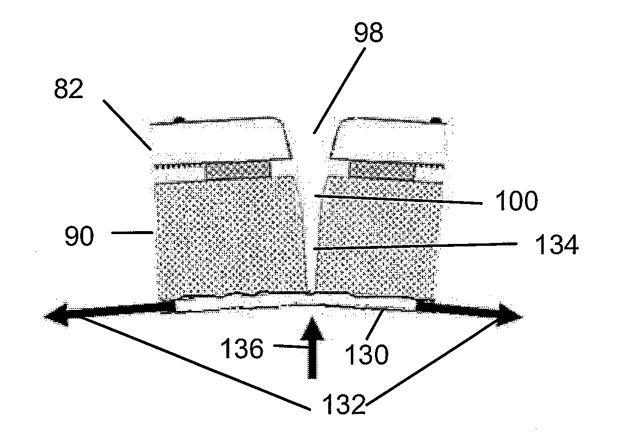
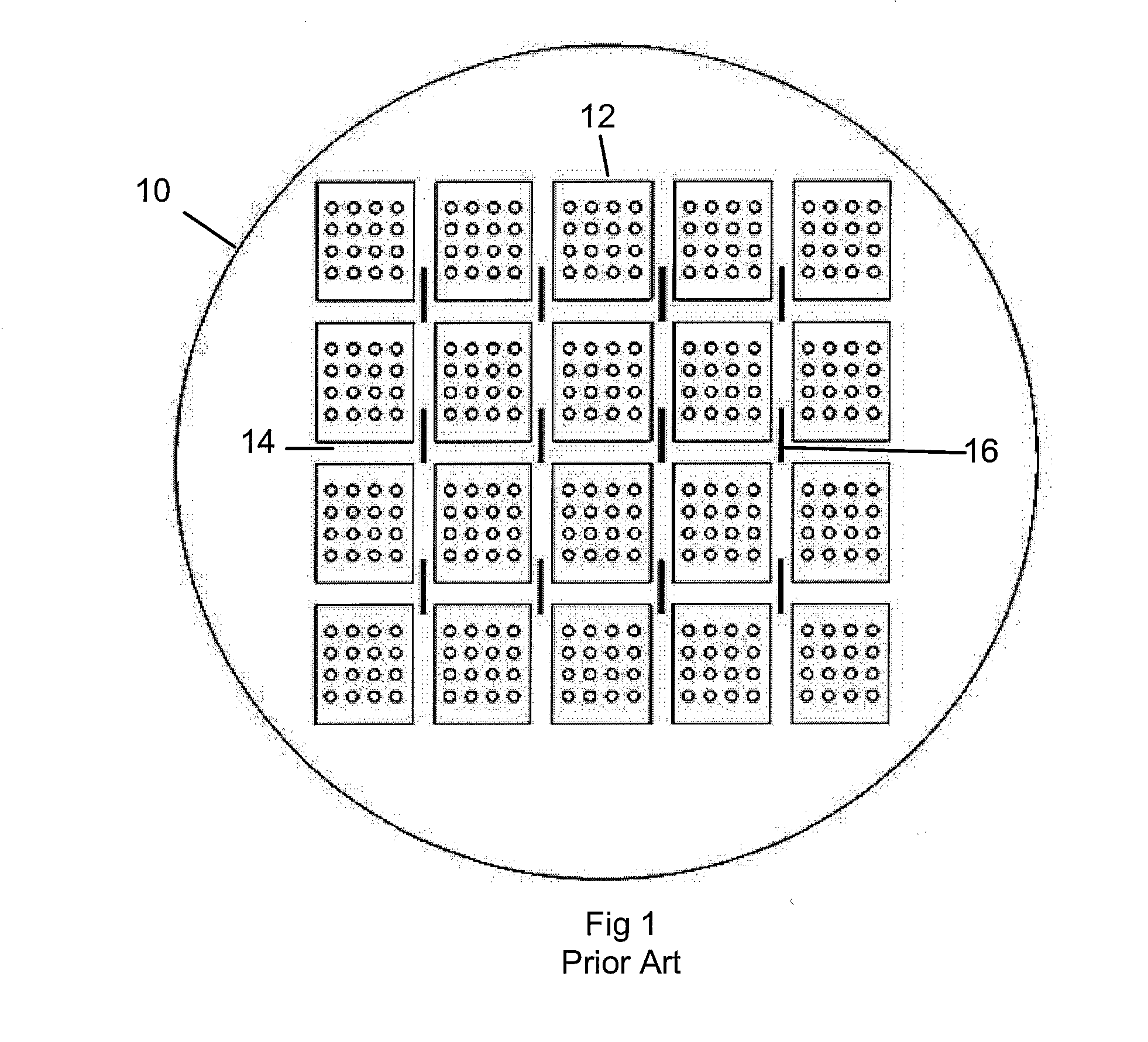
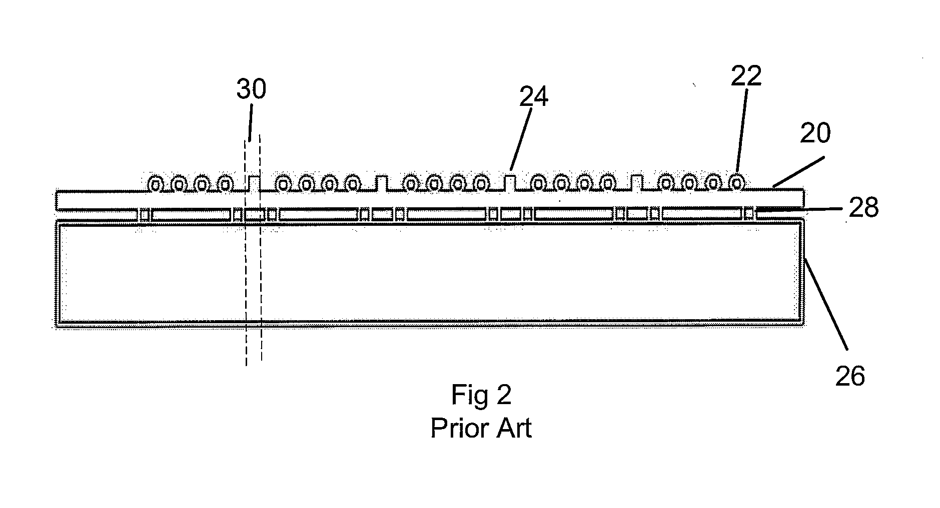
[0033]One object of the instant invention is to provide a method for singulation of compound electronic devices. Another object of the instant invention is to provide a method for singulation of compound electronic devices that avoids creating cracks or chips while maintaining acceptable cutting speeds. A further object of the instant invention is to provide a method for singulation of compound electronic devices that minimizes the size of streets. Compound electronic devices are particularly difficult to singulate due to their construction with two or more substrates requiring simultaneous separation to perform singulation. In particular, image sensor devices typically contain both active electronic device substrates such as silicon and transparent protective substrates made of glass or glass-like material, typically with differing thicknesses. One embodiment of the invention disclosed herein uses different separation techniques for different layers in the compound semiconductor de...


PUM

PropertyMeasurementUnit
wavelengthaaaaaaaaaa

Abstract

An improved method for singulation of compound electronic devices is presented. Compound electronic devices are manufactured by combining two or more substrates into an assembly containing multiple devices. Presented are methods for singulation of compound electronic devices using laser processing. The methods presented provide fewer defects such as cracking or chipping of the substrates while minimizing the width of the kerf and maintaining system throughput.

Description

TECHNICAL FIELD [0001]The present invention relates to singulation of electronic devices. In particular it relates to singulation of compound electronic devices, where the devices are constructed by assembling layers of potentially dissimilar substrates. In more particular it relates to singulation of image sensor compound semiconductor devices that comprise a substrate or wafer, often silicon, containing active circuit elements combined with an optically transparent protective substrate, often glass or sapphire.BACKGROUND [0002]Semiconductor and other electronic devices are typically manufactured by creating multiple copies of a device together on a substrate and then singulating the devices. Substrates can be comprised of silicon, sapphire, ceramic, glass or glass-like material. Singulation is the act of separating multiple devices manufactured on a substrate from each other by creating a cut or break between the devices to form individual devices. Singulation can be performed in ...

Claims


Application Information

Patent Timeline
Patent Type & Authority Applications(United States)
IPC IPC(8): H01L21/78
CPCB23K26/0635B23K26/367B23K2203/16B23K26/4075B23K2201/40B23K26/38B23K26/364B23K26/0624B23K26/40B23K2101/40B23K2103/16B23K2103/50H01L21/78H01L21/76
Inventor PIROGOVSKY, PETERALBELO, JEFFERY A.O'BRIEN, JAMESOSAKO, YASU
Owner ELECTRO SCI IND INC
Why Eureka
Try Eureka