Electron emitting element, electron emitting device, light emitting device, image display device, air blowing device, cooling device, charging device, image forming apparatus, electron-beam curing device, and method for producing electron emitting element

Active Publication Date: 2010-11-04
SHARP KK
View PDF41 Cites 45 Cited by
  • Summary
  • Abstract
  • Description
  • Claims
  • Application Information

AI Technical Summary

Benefits of technology

[0025]Further, in the electron emitting element, because the conductor having a high resistance to oxidation is used as the electrically conductive fine particles, element degradation is difficult to occur due to oxidization caused by oxygen in the atmosphere. This allows the electron emitting element to steadily work in the atmosphere.
[0026]Further, the insulating material and the electrically conductive fine particles can control an amount of ballistic electrons produced and a resistance value in the electron acceleration layer. This allows controlling a current value in the electron acceleration layer and an amount of electrons emitted. Moreover, the insulating material can also serve to effectively dissipate Joule heat generated by current flowing in the electron acceleration layer. This prevents the electron emitting element from being damage

Problems solved by technology

This changes an electric property of a semiconductor and reduces an electron emission current, which is a new problem.
In particular, deterioration of the semiconductor due to oxidation caused by oxygen in the atmosphere is inevitable, which is a serious problem.
However, if the thin metal film is too thin, a barrier effect against gas molecules is barely provided because it becomes difficult to form a dense film.
This causes a problem such that electron emission current decreases.
As a result, regarding the electron emitting elem

Method used


Image

  • Electron emitting element, electron emitting device, light emitting device, image display device, air blowing device, cooling device, charging device, image forming apparatus, electron-beam curing device, and method for producing electron emitting element
  • Electron emitting element, electron emitting device, light emitting device, image display device, air blowing device, cooling device, charging device, image forming apparatus, electron-beam curing device, and method for producing electron emitting element
  • Electron emitting element, electron emitting device, light emitting device, image display device, air blowing device, cooling device, charging device, image forming apparatus, electron-beam curing device, and method for producing electron emitting element

Examples


embodiment 1

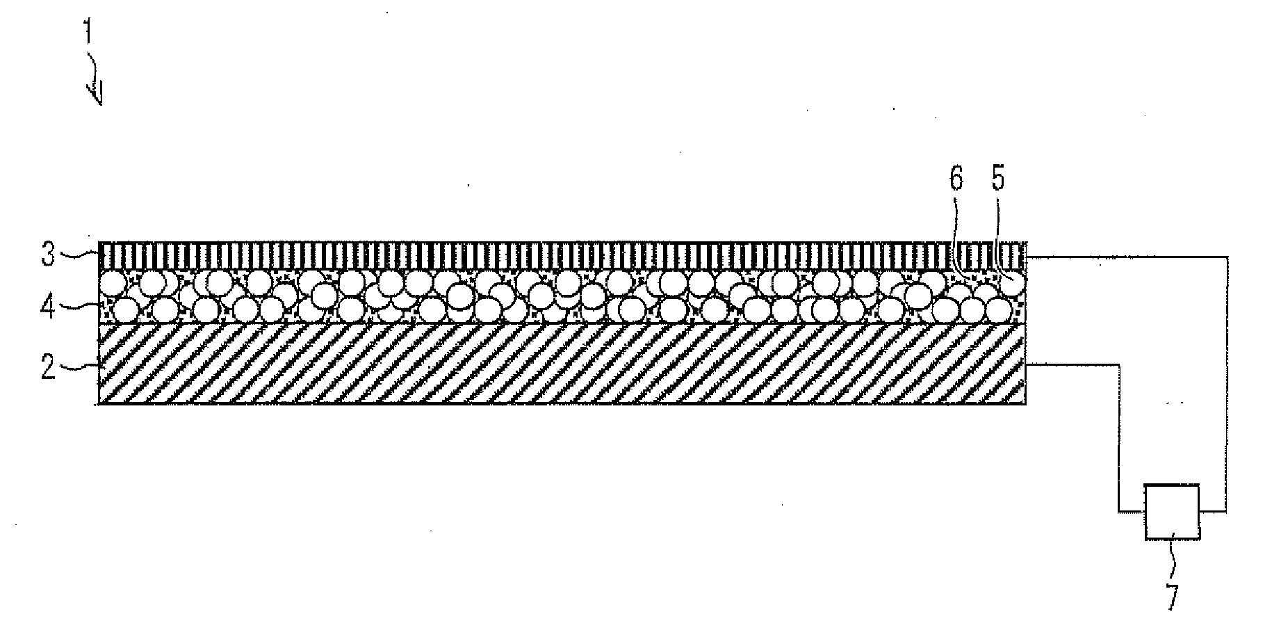
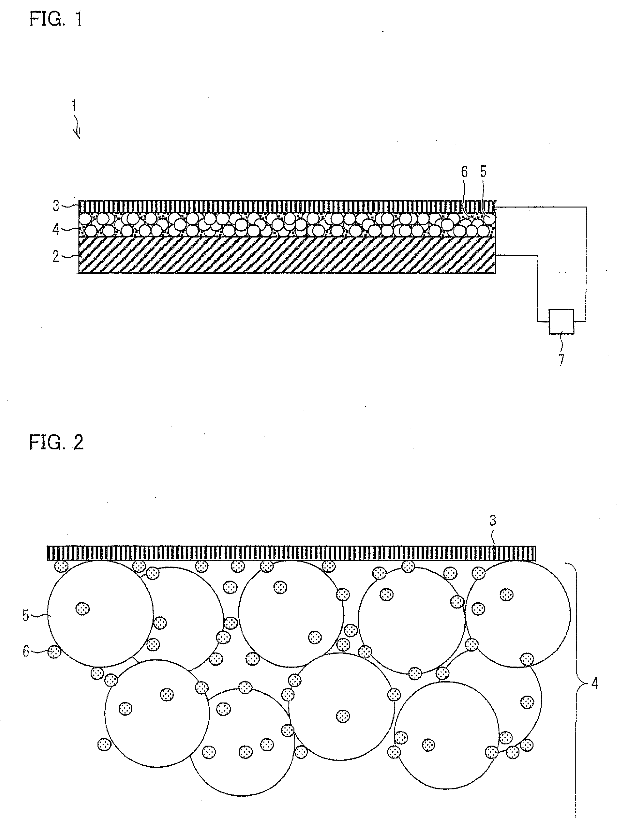
[0076]FIG. 1 is a schematic view illustrating an embodiment of an electron emitting element of the present invention. As illustrated in FIG. 1, an electron emitting element 1 of the present embodiment includes a substrate (electrode substrate) 2 serving as a lower electrode, an upper electrode (thin-film electrode) 3, and an electron acceleration layer 4 sandwiched between the substrate2 and the upper electrode 3. Further, the substrate 2 and the upper electrode 3 are connected to a power supply 7, so that a voltage can be applied between the substrate 2 and the upper electrode 3 which are provided so as to face each other. The electron emitting element 1 applies a voltage between the substrate 2 and the upper electrode 3 so that current flows between the substrate 2 and the upper electrode 3, that is, in the electron acceleration layer 4. A part of electrons in the current are caused to transmit through the upper electrode 3 or be emitted through gaps in the upper electrode 3 as ba...

example 1

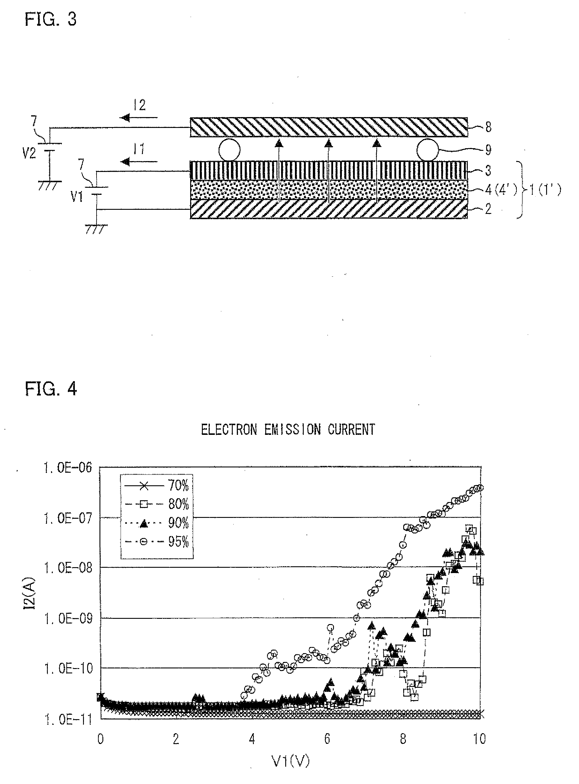
[0094]The following explanation deals with an example of an electron emission experiment by use of the electron emitting element of the present invention, with reference to FIG. 3 through FIG. 7. This experiment is merely an example of the present embodiment and by no means limits the present invention.

[0095]In the present example, five different kinds of electron emitting elements 1 were produced so that each electron emitting element 1 had a different composition of the insulating fine particles 5 and the metal fine particles 6 whose surfaces an insulating material (adhering substance) was attached to in the fine particle layer 4.

[0096]A 30 mm square SUS substrate was used as the substrate 2. On this substrate 2, the fine particle layer 4 was formed by the spin coating method. A solution used in the spin coating method was a solution which included the insulating fine particles 5 and the metal fine particles 6 whose surfaces an insulating material was attached to. The solution was...

example 2

[0107]In the present example, four kinds of electron emitting elements 1 were produced so that, while compositions of the insulating fine particles 5 and the metal fine particles 6 whose surfaces an insulating material was attached to were the same as those in Example 1, a layer thickness of the fine particle layer 4 was changed by changing condition for film formation of the fine particle layer 4.

[0108]Regarding the insulating fine particles 5 and the metal fine particles 6 which were dispersed in a dispersion solution to be used in spin coating, a composition ratio of the insulating fine particles 5 and the metal fine particles 6 whose surfaces an insulating material was attached to was adjusted such that a ratio by weight of the insulating fine particles 5 with respect to the total amount of the insulating fine particles 5 and the metal fine particles 6 was 80%. Film formation under the above described condition for film formation was carried out once or five times according to t...


PUM


Abstract

An electron emitting element (1) includes a substrate (2), an upper electrode (3), and a fine particle layer (4) sandwiched between the substrate (2) and the upper electrode (3). The fine particle layer (4) includes metal fine particles (6) with high resistance to oxidation, and insulating fine particles (5) larger in size than the metal fine particles (6). The electron emitting element (1) can steadily emit electrons not only in vacuum but also in the atmosphere. Further, the electron emitting element (1) can work without electric discharge so that harmful substances such as ozone, NOx, or the like are scarcely generated. Accordingly, degradation of the electron emitting element (1) due to oxidation does not occur. Therefore, the electron emitting element (1) has a long life and can steadily work continuously for a long period of time even in the atmosphere.

Description

TECHNICAL FIELD [0001]The present invention relates to an electron emitting element for emitting electrons by application of a voltage.BACKGROUND ART[0002]A Spindt-type electrode and a carbon nanotube electrode (CNT) have been known as conventional electron emitting elements. Applications of such conventional electron emitting elements to, for example, the field of Field Emission Display (FED) have been studied. Such electron emitting elements are caused to emit electrons by tunnel effect resulting from formation of an intense electric field of approximately 1 GV / m that is produced by application of a voltage to a pointed section.[0003]Conventionally, it has been desired that an electron emitting element works in the atmosphere, and there has been an idea of, for example, applying such an electron emitting element to a charging device or an electrostatic latent image forming device. As for an example of an electron emitting element using the Spindt-type electrode, an electron emitti...

Claims


Application Information

Patent Timeline
IPC IPC(8): G03G15/02H01J1/02H05B41/00H05F3/00H01J9/00
CPCB82Y10/00G03G15/0233G02F2001/133625H01J1/312H01J63/02G03G15/0258G02F1/133625
Inventor KANDA, HIROFUMIIWAMATSU, TADASHITAMURA, TOSHIHIROHIRAKAWA, HIROYUKIICHII, YOSHIO
Owner SHARP KK
Why Eureka
Try Eureka