
Display device and drive method thereof

a display device and active matrix technology, applied in the field of active matrix display devices and drive methods thereof, can solve the problems of tfts experiencing a change in off characteristics, and achieve the effects of reducing the amount of charge accumulated, and reducing the production cost of liquid crystal display devices

Inactive Publication Date: 2011-01-20
SHARP KK
View PDF13 Cites 7 Cited by
  • Summary
  • Abstract
  • Description
  • Claims
  • Application Information

AI Technical Summary

Benefits of technology

[0038]According to the first and tenth aspects of the present invention, the scanning signal line driver circuit applies a predetermined pulse, which has the same polarity as an off voltage for the switching element and is at a higher level than the off voltage, to each scanning signal line during a period in which the scanning signal line is not active. Accordingly, it is possible to eliminate more charge accumulated in the vicinity of the switching element due to a long period of conduction to the display device. Thus, the display device can suppress characteristic changes of the switching element, thereby achieving high-quality video display.
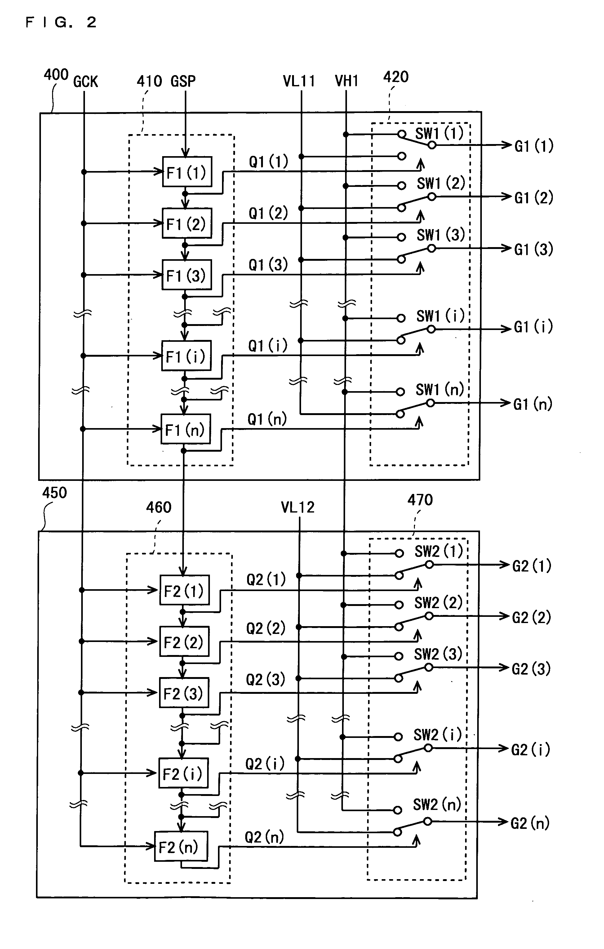
[0039]According to the second aspect of the present invention, the predetermined pulse is applied to the second scanning signal line group when the first scanning signal line group is active and to the first scanning signal line group when the second scanning signal line group is active. In this case, the first scanning signal line driver circuit for activating the first scanning signal line group and the second scanning signal line driver circuit for activating the second scanning signal line group can be separately configured by individual IC chips, and therefore existing scanning signal line driver circuits can be diverted. Thus, it is possible to minimize production cost of the liquid crystal display device.
[0040]According to the third aspect of the present invention, the predetermined pulse is applied to the scanning signal lines and the activation pulse is applied to activate the scanning signal lines. In this case, the predetermined pulse is applied to each of the scanning signal lines immediately before application of the activation pulse, and therefore the display device can hold a voltage corresponding to video to be displayed in the pixel formation portion with a charge accumulated in the vicinity of the switching element being eliminated. Thus, it is possible to suppress characteristic changes of the switching element, thereby achieving higher-quality video display.
[0041]According to the fourth aspect of the present invention, the predetermined pulse is applied multiple times before application of the activation pulse. As a result, the period in which to apply the predetermined pulse is extended, making it possible to eliminate more charge accumulated in the vicinity of the switching element. Consequently, further higher-quality video display can be achieved.
[0042]According to the fifth aspect of the present invention, the predetermined pulse having a pulse width of one horizontal period or more is applied, making it possible to eliminate more charge accumulated in the vicinity of the switching element.
[0043]According to the sixth aspect of the present invention, it is possible to turn the switching element on when the first voltage is applied and off when the second voltage is applied, and also possible to eliminate a charge accumulated in the vicinity of the switching element when the third voltage is applied.

Problems solved by technology

However, if the liquid crystal display device, which has a liquid crystal panel provided therein, is subjected to a long period of conduction, TFTs experience a change in off characteristics.
In this case, the gate-off voltage needs to be set considering the fall of the blurring voltage, resulting in inconveniences such as the need to enhance a withstanding voltage of a gate driver.

Method used


Image

  • Display device and drive method thereof
  • Display device and drive method thereof
  • Display device and drive method thereof

Examples


first embodiment

1. First Embodiment

1.1 Overall Configuration and Operation

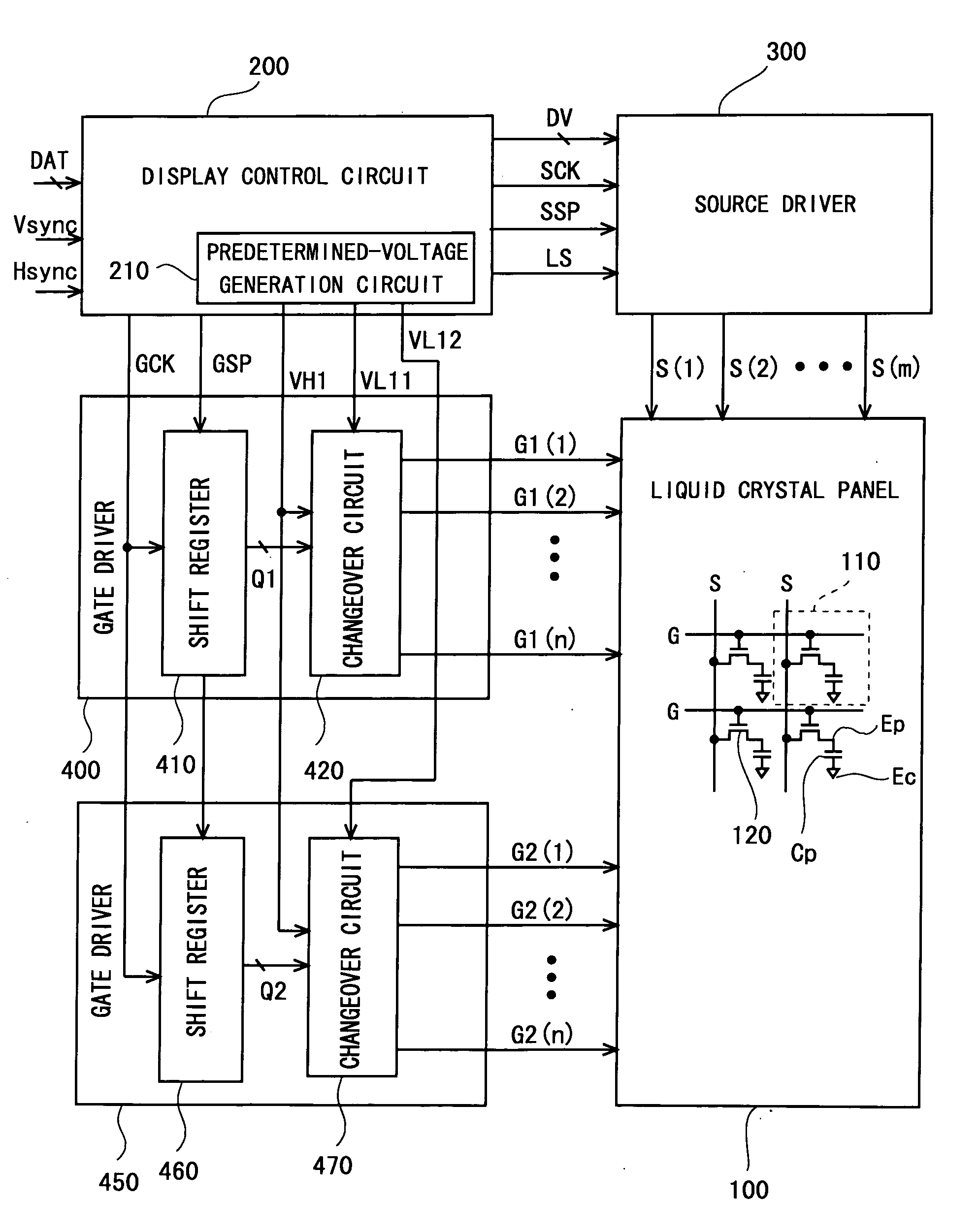
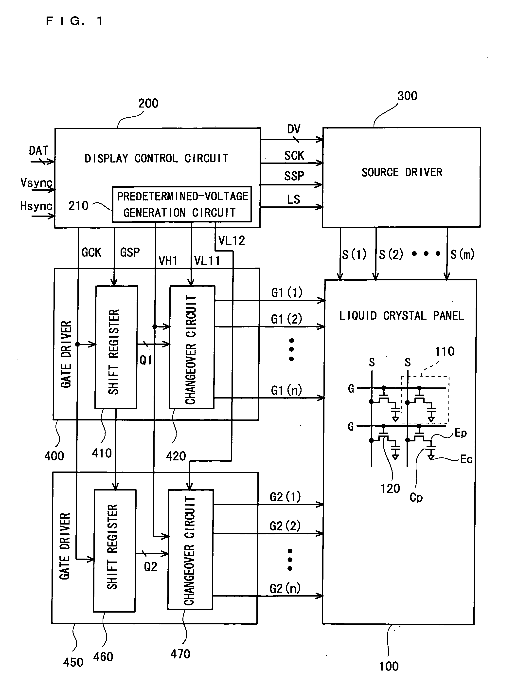
[0070]FIG. 1 is a block diagram illustrating the overall configuration of an active-matrix liquid crystal display device according to a first embodiment of the present invention. The liquid crystal display device is provided with a liquid crystal panel 100, a display control circuit 200, a source driver (video signal line driver circuit) 300, a first gate driver (scanning signal line driver circuit) 400, and a second gate driver 450.

[0071]The liquid crystal panel 100 includes a plurality (m) of video signal lines S1 to Sm and a plurality (2n) of scanning signal lines G1(1) to G1(n) and G2(1) to G2(n). Of the 2n scanning signal lines, the scanning signal lines G1(n) to G1(n) are driven by the first gate driver 400, while the scanning signal lines G2(1) to G2(n) are driven by the second gate driver 450.

[0072]The liquid crystal panel 100 further includes a plurality (m×2n) of pixel formation portions 110 provided at their respec...

second embodiment

2. Second Embodiment

2.1 Overall Configuration and Operation

[0099]FIG. 7 is a block diagram illustrating the overall configuration of an active-matrix liquid crystal display device according to a second embodiment of the present invention. Elements of the liquid crystal display device that are the same as those of the liquid crystal display device according to the first embodiment are denoted by the same reference characters and any descriptions thereof will be omitted.

[0100]Unlike in the first embodiment, the 2n scanning signal lines G(1) to G(2n) included in the liquid crystal panel 100 of the liquid crystal display device are driven by a gate driver 500. The gate driver 500 is made up of a shift register 510 and a changeover circuit 520. The shift register 510 sequentially outputs pulse signals Q(1) to Q(2n) to the changeover circuit 520 based on the gate start pulse signal GSP and the gate clock signal GCK outputted by the display control circuit 200. Based on the pulse signals Q...

third embodiment

3. Third Embodiment

3.1 Overall Configuration and Operation

[0120]FIG. 11 is a block diagram illustrating the overall configuration of an active-matrix liquid crystal display device according to a third embodiment of the present invention. Elements of the liquid crystal display device that are the same as those of the liquid crystal display device according to the second embodiment are denoted by the same reference characters, and any descriptions thereof will be omitted.

[0121]Unlike in the second embodiment, the liquid crystal display device is driven by a gate driver 600 provided with a plurality (3n) of scanning signal lines G(1) to G(3n) in the liquid crystal panel 100. The gate driver 600 is made up of a shift register 610, an AND circuit 630, and a changeover circuit 620. The shift register 610 sequentially outputs pulse signals Q(1) to Q(3) to the AND circuit 630 based on a gate start pulse signal GSP and a gate clock signal GCK outputted by the display control circuit 270. The...


PUM


Abstract

A display device is disclosed which is capable of suppressing characteristic changes due to a long period of conduction, thereby achieving high-quality video display, and also to provide a drive method therefor. In at least one embodiment, while sequentially activating n first scanning signal line groups G1(1) to G1(n), a predetermined voltage, which is the same as a voltage for turning off a thin-film transistor included in each pixel formation portion in that the polarity thereof is negative and is at a higher level than that voltage, is applied simultaneously to n second scanning signal line groups G2(1) to G2(n). Thereafter, while sequentially activating the n second scanning signal line groups G2(1) to G2(n), the predetermined voltage is applied simultaneously to the n first scanning signal line groups G1(1) to G1(n). By repeating this, charges accumulated in the vicinity of the thin-film transistors are eliminated, thereby suppressing changes in off characteristics thereof. At least one embodiment of the present invention is suitable for matrix display devices intended for a long period of use.

Description

TECHNICAL FIELD[0001]The present invention relates to active-matrix display devices and drive methods thereof, more particularly to an active-matrix display device and a drive method therefor in which characteristic changes resulting from a long period of conduction are suppressed.BACKGROUND ART[0002]As displays for television, personal computer, etc., active-matrix liquid crystal display devices have been used which are capable of high-quality video display. Liquid crystal display devices include pixel formation portions each being provided with a thin film transistor (hereinafter, referred to as a “TFT”) and a pixel electrode. In the case where the TFT is on, when a potential corresponding to video to be displayed is applied to the pixel electrode through a video signal line via the TFT, a voltage (gate-off voltage) for turning off a gate of the TFT is applied to the gate until another potential corresponding to the next video to be displayed is applied. As a result, the TFT is ma...

Claims


Application Information

Patent Timeline
Patent Type & Authority Applications(United States)
IPC IPC(8): G09G5/10
CPCG09G3/20G09G2370/08G09G2310/08G09G2310/0256
Inventor MORIMOTO, TAKASHI
Owner SHARP KK
Learn More