Touch display panel

Active Publication Date: 2011-06-23
AU OPTRONICS CORP
View PDF10 Cites 56 Cited by
  • Summary
  • Abstract
  • Description
  • Claims
  • Application Information

AI Technical Summary

Benefits of technology

[0008]The invention provides a touch display panel which

Problems solved by technology

However, the transparent conductive material has

Method used


Image

  • Touch display panel
  • Touch display panel
  • Touch display panel

Examples


first embodiment

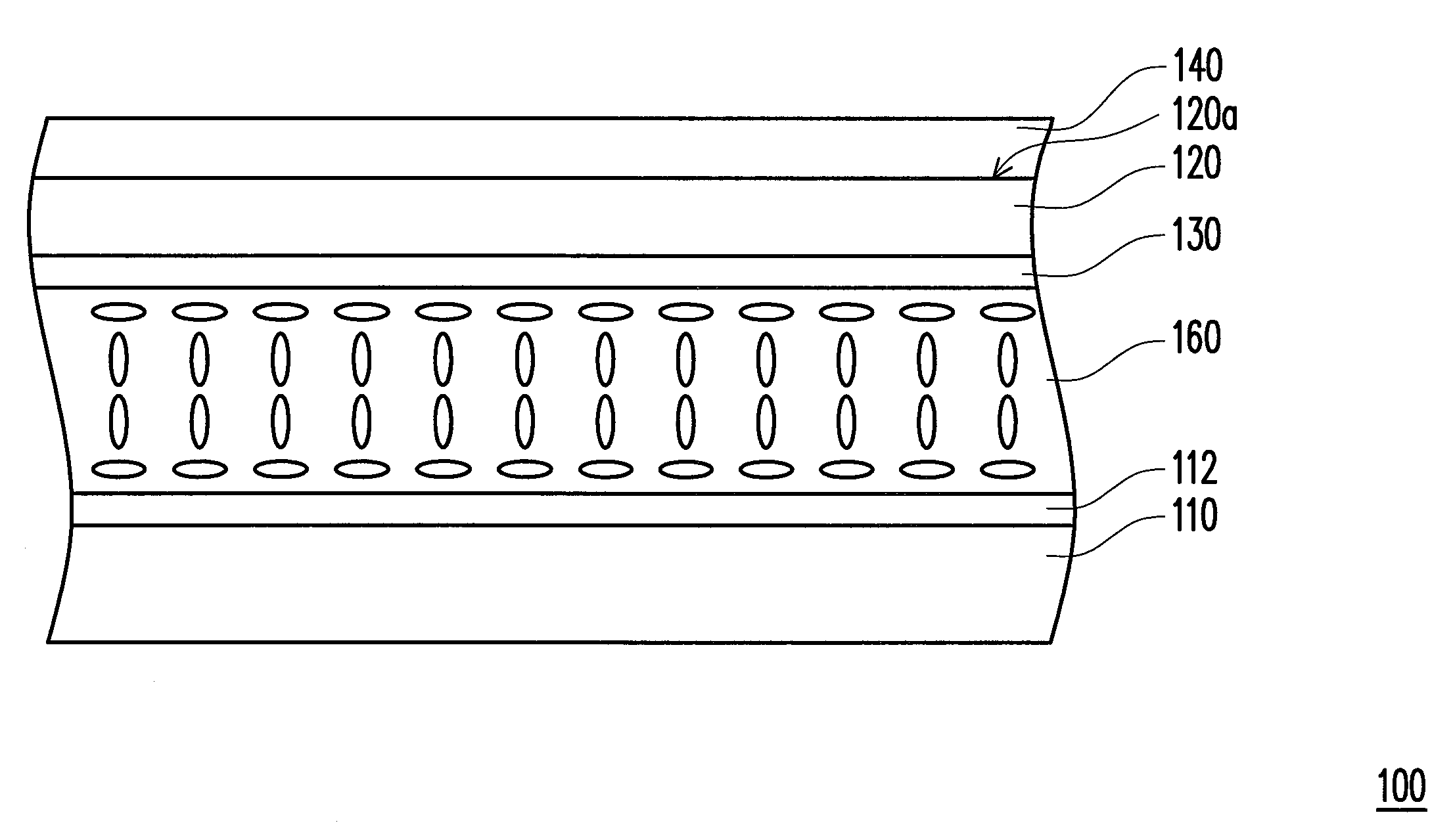
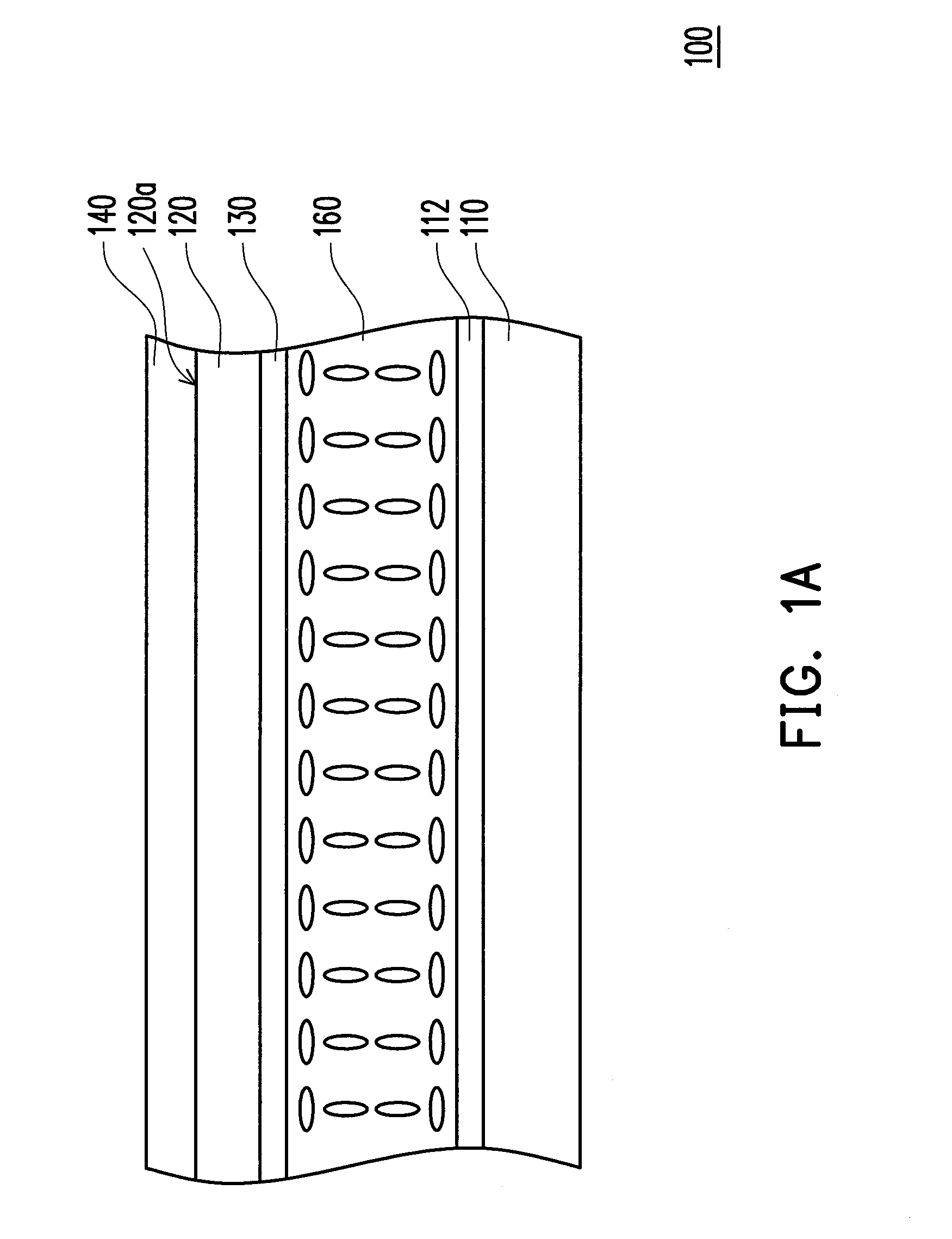
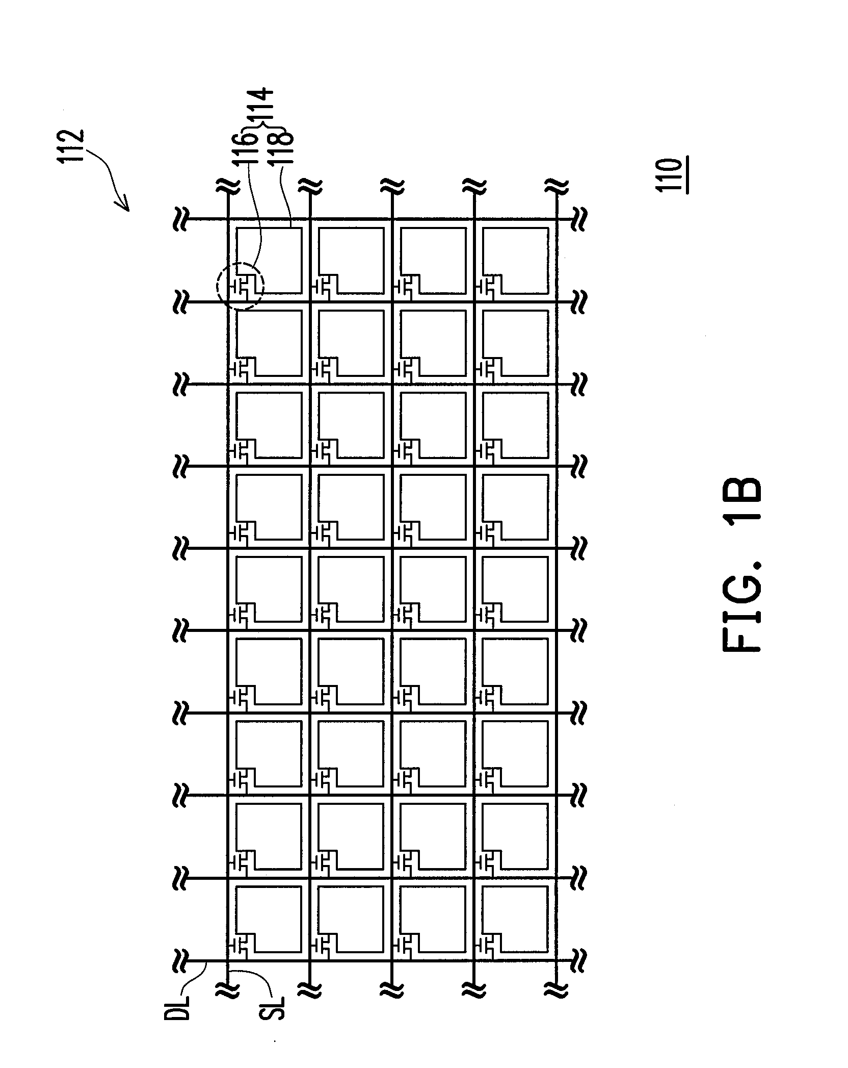
[0053]FIG. 1A is a schematic cross-sectional view of a touch display panel according to a first embodiment of the present invention, FIG. 1B is a schematic top view of the first substrate 110 depicted in FIG. 1A, FIG. 1C is a schematic top view of the light shielding pattern layer 130 depicted in FIG. 1A, FIG. 1D is a schematic top view of the touch sensing layer 140 depicted in FIG. 1A, FIG. 1E is a schematic drawing showing the relation between the mesh touch pad 146 and the light shielding pattern layer 130, and FIG. 1F is a schematic drawing showing the relation between the grid pattern 148 and the pixel unit 132 depicted in FIG. 1E.

[0054]Referring to FIG. 1A, a touch display panel 100 includes a first substrate 110, a second substrate 120, a light shielding pattern layer 130, a touch sensing layer 140, and a display medium 160. The second substrate 120 is disposed opposite to the first substrate 110. The display medium 160 is sandwiched between the first substrate 110 and the s...

second embodiment

[0063]FIG. 2A is a schematic top view of a mesh touch pad 146a of a touch display panel according to a second embodiment of the present invention, FIG. 2B is a schematic drawing showing the relation between the mesh touch pad 146a and the light shielding pattern layer 130, and FIG. 2C is a schematic drawing showing the relation between the grid pattern 148a and the pixel unit 132 depicted in FIG. 2B.

[0064]Referring to FIG. 2A, FIG. 2B and FIG. 2C, in the embodiment, the grid pattern 148a of the mesh touch pad 146a is quadrangle-shaped, and an angle θ between the bottom edge 150 of the quadrangle-shaped grid pattern 148a and the pixel edge PL of the pixel unit 132 is 0°. More specifically, the grid pattern 148a is square-shaped, for example, and the grid edge length GL is less than ⅛ of the pixel edge length PL of the pixel unit 132. If the pixel edge length PL is 200 μm for example, the grid edge length GL of the quadrangle-shaped grid pattern 148a is 5˜25 μm, and preferably is 25 μ...

third embodiment

[0067]FIG. 3A is a schematic top view of a mesh touch pad 146b of a touch display panel according to a third embodiment of the present invention, FIG. 3B is a schematic drawing showing the relation between the mesh touch pad 146b and the light shielding pattern layer 130, and FIG. 3C is a schematic drawing showing the relation between the grid pattern 148b and the pixel unit 132 depicted in FIG. 3B.

[0068]Referring to FIG. 3A, FIG. 3B and FIG. 3C, in the embodiment, the grid pattern 148b of the mesh touch pad 146b is hexagon-shaped, and an angle θ between the bottom edge 150 of the hexagon-shaped grid pattern 148b and the pixel edge PL of the pixel unit 132 is 10˜45°, and preferably is 45°. More specifically, the grid pattern 148b is hexagon-shaped, for example, and the grid edge length GL is less than ⅙ of the pixel edge length PL of the pixel unit 132. If the pixel edge length PL is 200 μm for example, the grid edge length GL of the hexagon-shaped grid pattern 148b is 5˜33 μm, and ...


PUM


Abstract

A touch display panel including a first substrate, a second substrate, a light shielding pattern layer, a touch sensing layer and a display medium is provided. The light shielding pattern layer is disposed on the first substrate or the second substrate. Pixel units are defined by the light shielding pattern layer, each pixel unit has a pixel edge length, and each pixel unit is disposed corresponding to one of the pixel structures. The touch sensing layer is disposed on the second substrate and has a plurality of first touch series and a plurality of second touch series. Each first touch series and each touch series respectively have mesh touch pads serially connected to each other. Each mesh touch pad has a plurality of grid patterns, each grid pattern has a grid edge length, and the grid edge length is ⅛˜⅗ of the pixel edge length.

Description

CROSS-REFERENCE TO RELATED APPLICATION[0001]This application claims the priority benefit of Taiwan application serial no. 98144304, filed on Dec. 22, 2009. The entirety the above-mentioned patent application is hereby incorporated by reference herein and made a part of specification.BACKGROUND OF THE INVENTION[0002]1. Field of the Invention[0003]The present invention relates to a display panel, and particularly relates to a touch display panel.[0004]2. Description of Related Art[0005]In current information era, human beings by degrees tend to rely on electronic products. The electronic products such as mobile phones, handheld personal computers (PCs), personal digital assistants (PDAs) and smart phones have pervaded everywhere in our daily life. To meet current demands on portable, compact, and user-friendly information technology (IT) products, touch panels have been introduced as input devices in replacement of conventional keyboards or mice. Among the touch panels, a touch displa...

Claims


Application Information

Patent Timeline
IPC IPC(8): G06F3/041
CPCG06F3/0412G06F2203/04111G06F3/047G06F3/044G06F3/0443
Inventor CHEN, CHENG-ANKUO, WEI-HUNGYANG, TUN-CHUNLEE, SEOK-LYULHUANG, WEI-MING
Owner AU OPTRONICS CORP
Why Eureka
Try Eureka