

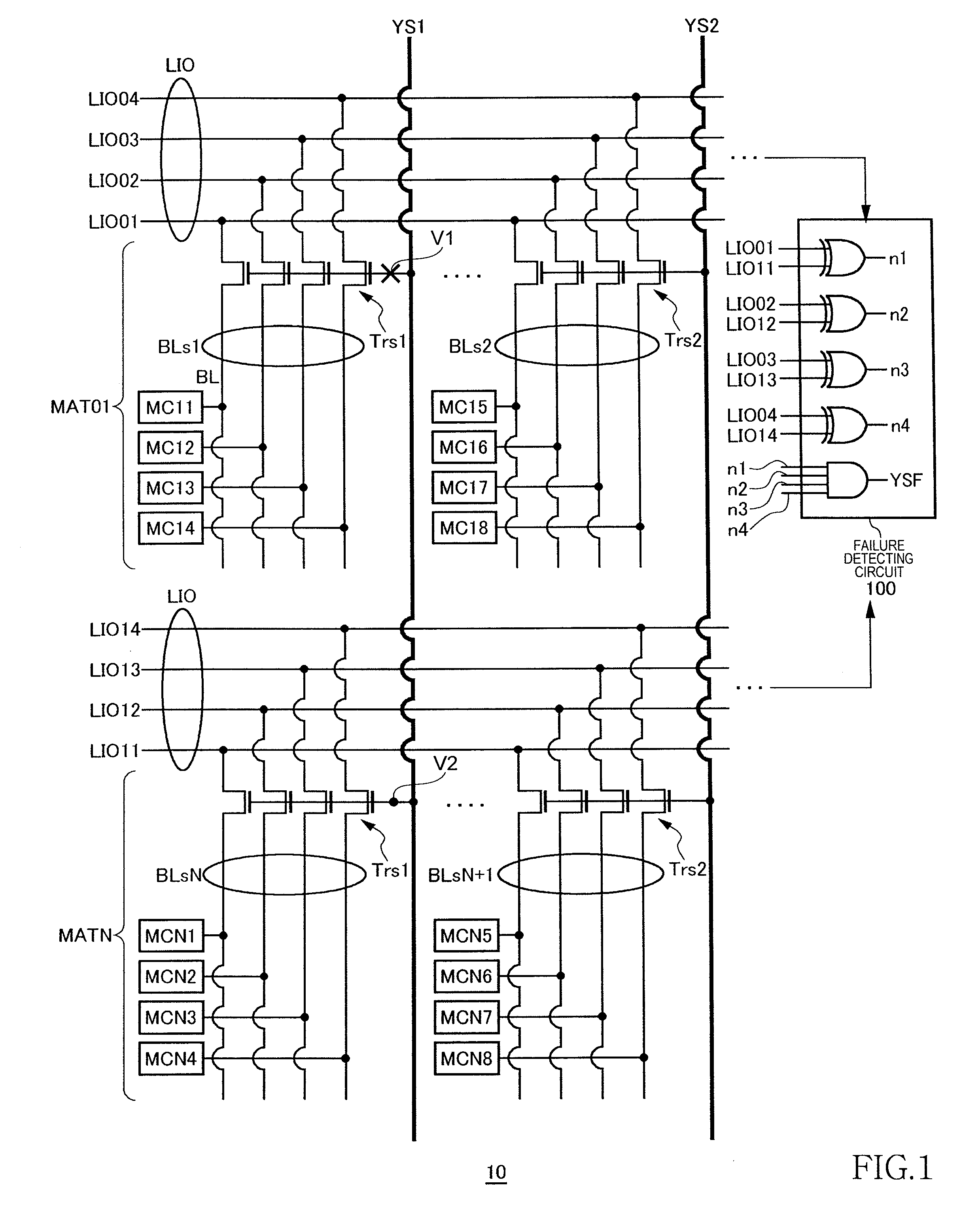
Semiconductor device having bit lines and local I/O lines
a technology of micro-i/o lines and semiconductor devices, which is applied in the direction of information storage, static storage, digital storage, etc., can solve the problems of high conductance resistance of these contact holes, contact failure, and replacement targets being likely to accidentally connect with local i/o lines, so as to facilitate efficient line failure discrimination
- Summary
- Abstract
- Description
- Claims
- Application Information
AI Technical Summary
Benefits of technology
Problems solved by technology
Method used
Image

Examples
embodiment
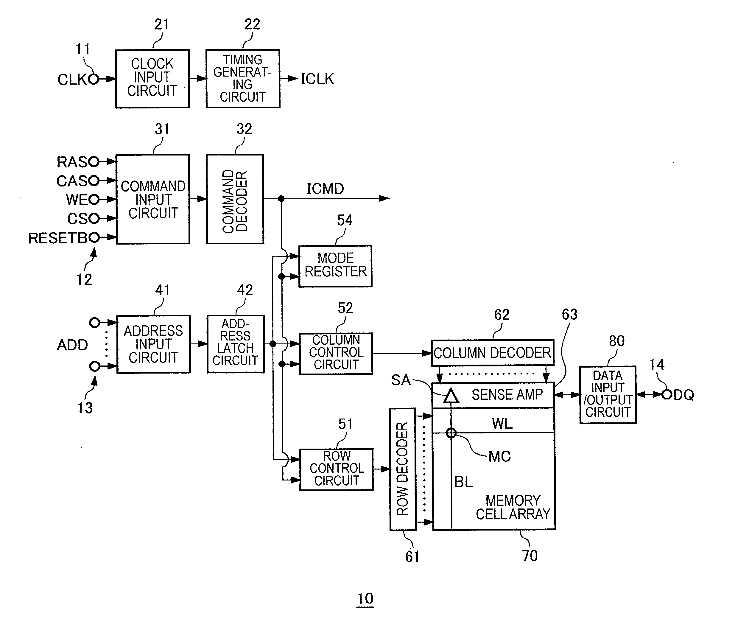
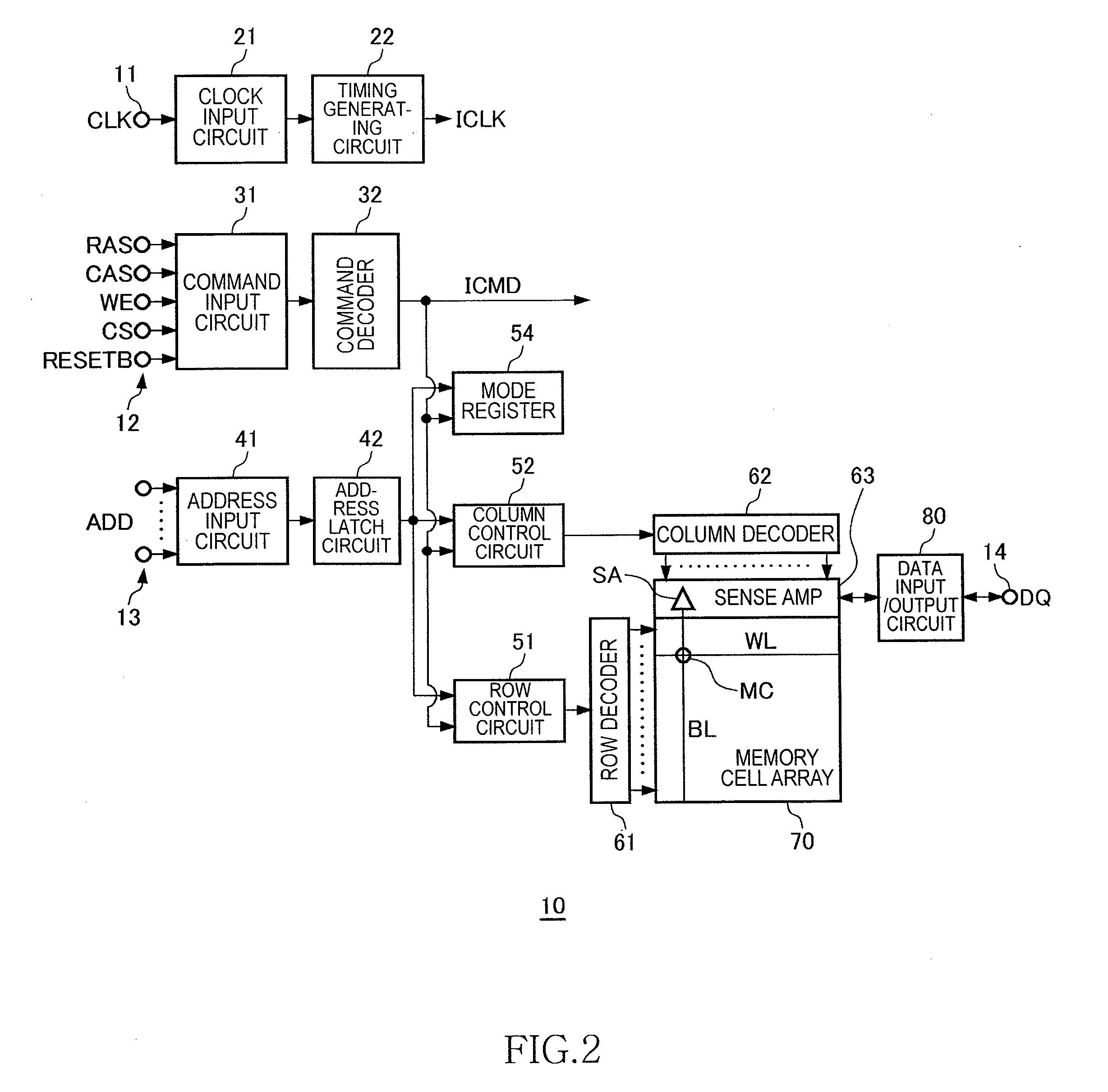
[0033]FIG. 2 is a functional block diagram of the semiconductor device 10. The semiconductor device 10 according to the present embodiment is a DDR (Double-Data-Rate) type SDRAM (Synchronous Dynamic Random Access Memory), and has a clock terminal 11, a command terminal 12, an address terminal 13 and a data input / output terminal 14 as external terminals. In addition, although a data strobe terminal and calibration terminal are also provided, these are not illustrated in figures.
[0034]The clock terminal 11 receives a clock signal CLK, and the supplied clock signal CLK is supplied to the clock input circuit 21. The output of the clock input circuit 21 is supplied to a timing generating circuit 22. The timing generating circuit 22 generates an internal clock ICLK to supply to various internal circuits which will be described below.
[0035]The command terminal 12 receives command signals such as a row address strobe signal RAS, a column address strobe signal CAS, a write enable signal WE, ...
PUM
 Abstract
Description
Claims
Application Information