LCD Device And LED Package Structure Thereof

a technology of liquid crystal display and led chip, which is applied in the field of display technologies, can solve problems such as poor light mixture performance, and achieve the effects of eliminating hot spot phenomenon, reducing light mixing distance, and avoiding light emission blind areas

Active Publication Date: 2013-06-06
TCL CHINA STAR OPTOELECTRONICS TECH CO LTD
View PDF15 Cites 2 Cited by
  • Summary
  • Abstract
  • Description
  • Claims
  • Application Information

AI Technical Summary

Benefits of technology

[0004]The primary objective of the present disclosure is to provide an LCD device and an LED package structure thereof that can eliminate the hot spot phenomenon.
[0025]The present disclosure has the following benefits as compared to the prior art: by disposing the LED chip on the bottom wall and having the first sidewall obliquely disposed in a light exiting direction of the LED chip, light rays emitted from the LED chip can be reflected by the first sidewall and exit from the light exiting wall. This can increase the light mixing distance for the LED chip and avoid occurrence of light emission blind areas, thus eliminating the hot spot phenomenon.

Problems solved by technology

This will further cause poor light mixture performance due to hot spots generated at the light incident side of the LCD device.

Method used


Image

  • LCD Device And LED Package Structure Thereof
  • LCD Device And LED Package Structure Thereof
  • LCD Device And LED Package Structure Thereof

Examples


first embodiment

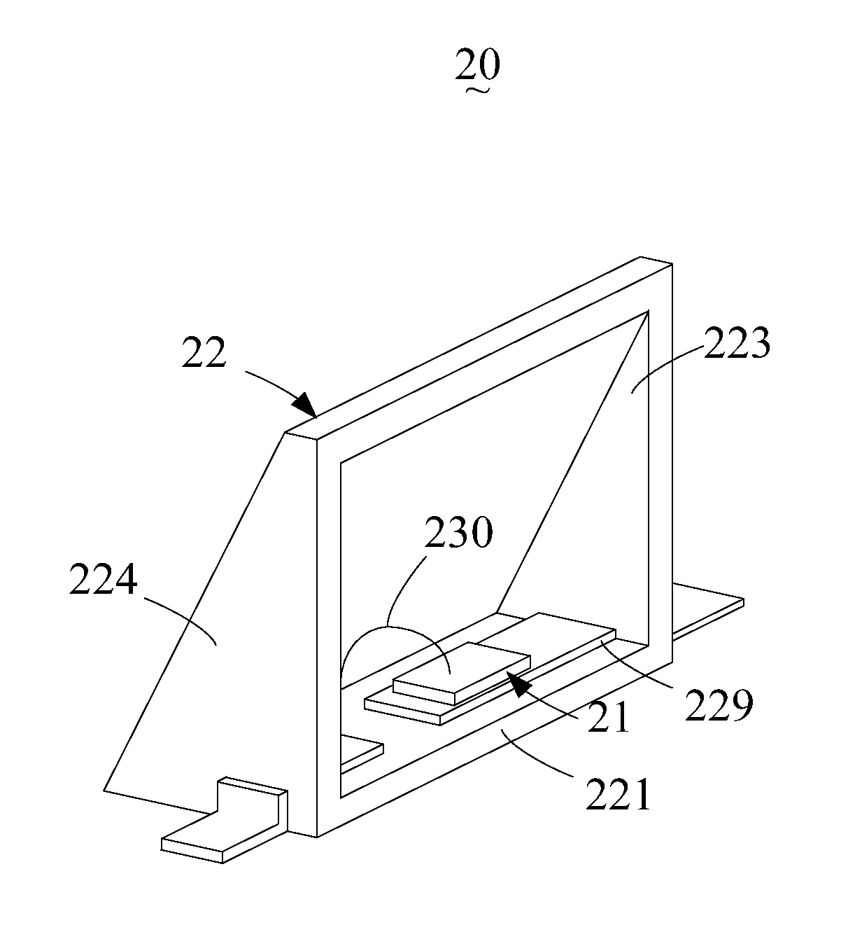
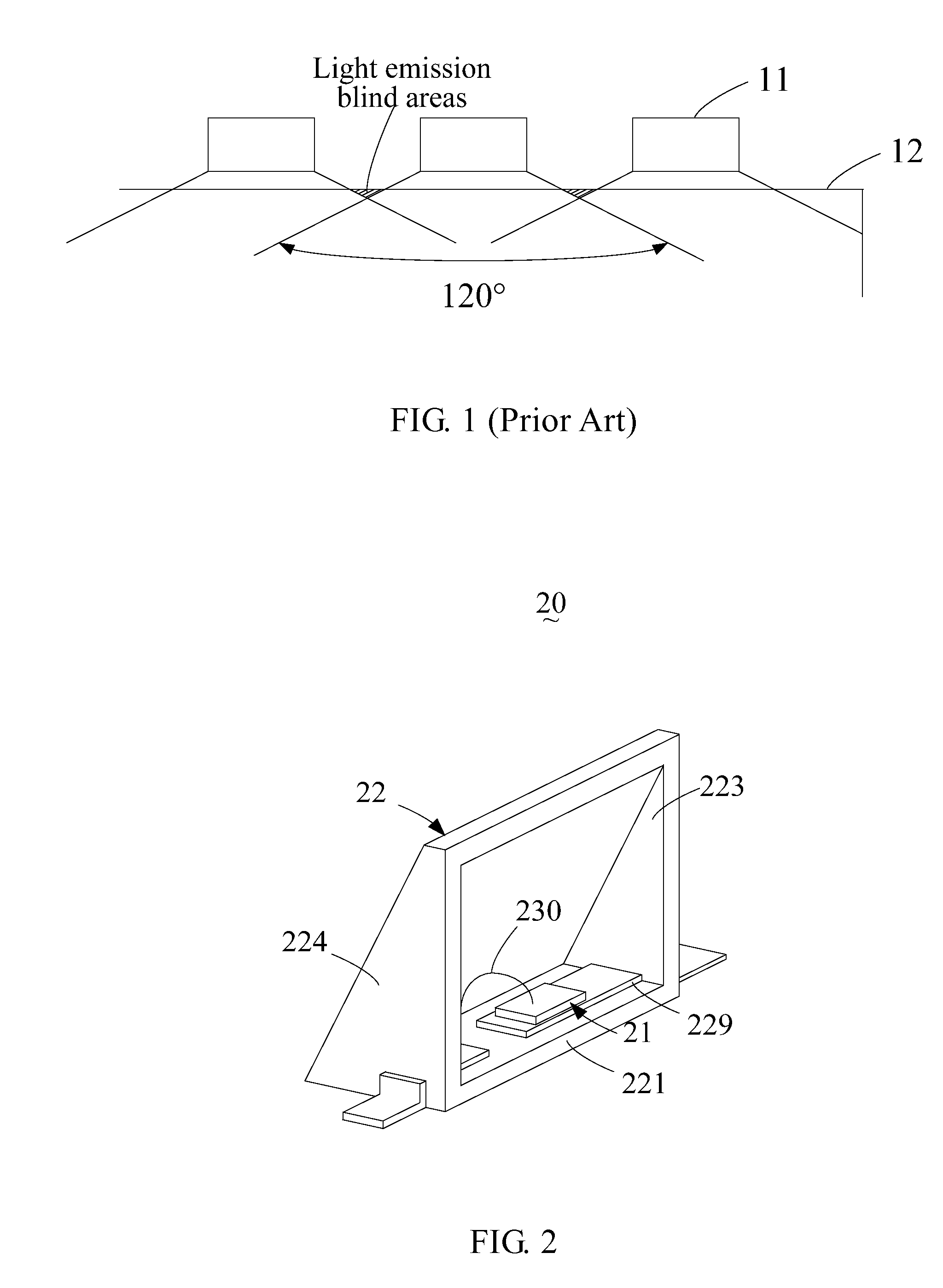
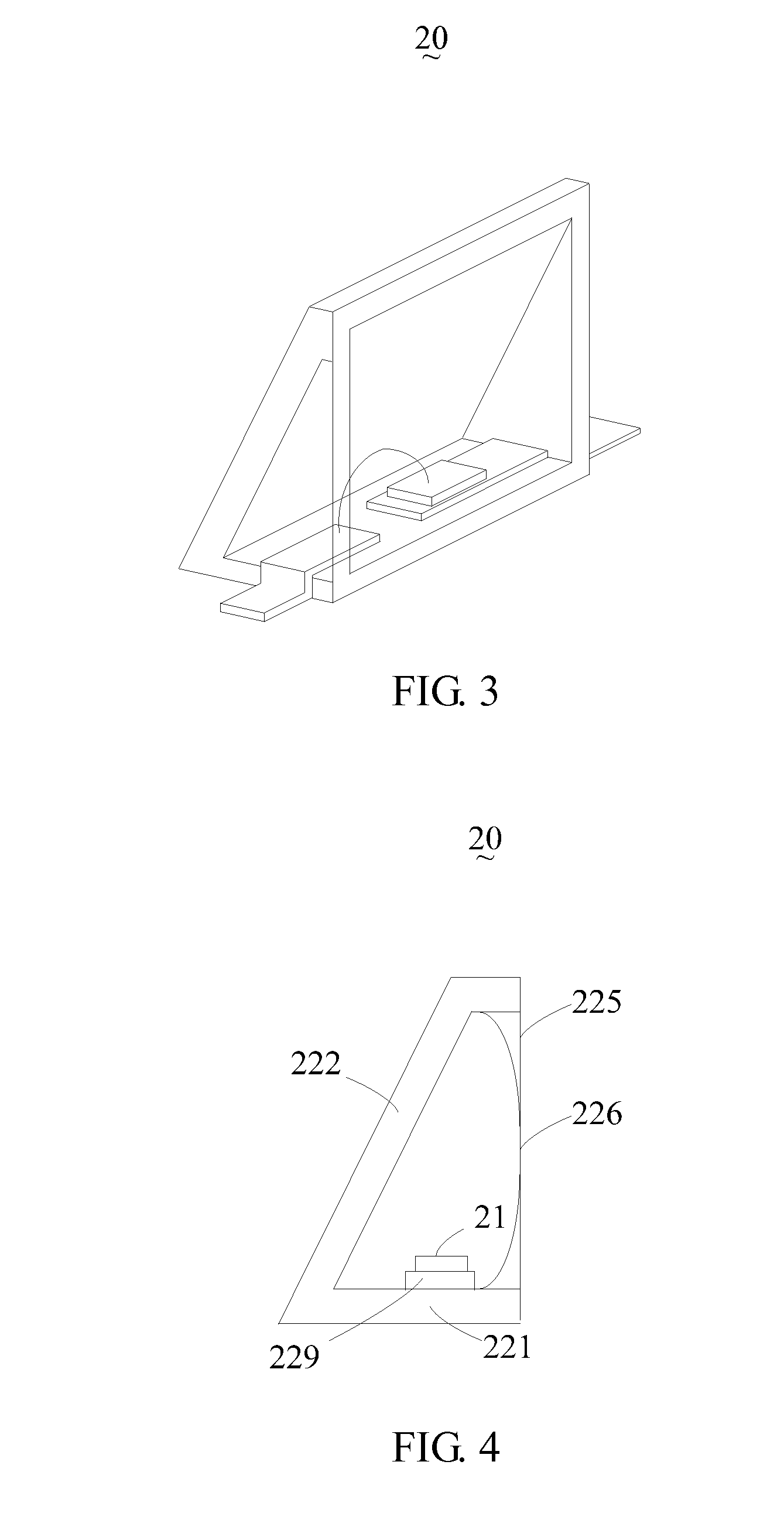
[0039]Referring to FIG. 2 to FIG. 4, FIG. 2 is a schematic perspective view of an LED package structure according to the present disclosure, FIG. 3 is a perspective view of the LED package structure in FIG. 2, and FIG. 4 is a schematic cross-sectional view of the LED package structure in FIG. 2. As shown in FIG. 2 to FIG. 4, the LED package structure 20 of this embodiment comprises: an LED chip 21 and a frame 22 for receiving the LED chip 21. The frame 22 comprises a bottom wall 221, a first sidewall 222, a second sidewall 223, a third sidewall 224, and a light exiting wall 225. The LED package structure 20 further comprises a soldering pin 229 and a wire 230.

[0040]In this embodiment, the soldering pin 229 is disposed on the bottom wall 221, and comprises a first soldering pin part and a second soldering pin part. The LED chip 21 is disposed on the first soldering pin part and is connected with the second soldering pin part via the wire 230; that is, the LED chip 21 is disposed on t...

third embodiment

[0045]Referring to FIG. 8 to FIG. 10, FIG. 8 is a schematic perspective view of an LED package structure according to the present disclosure, FIG. 9 is a perspective view of the LED package structure in FIG. 8, and FIG. 10 is a schematic cross-sectional view of the LED package structure in FIG. 8. As shown in FIG. 8 to FIG. 10, a light source module 40 of this embodiment comprises: an LED chip 41 and a frame 42 for receiving the LED chip 41. The frame 42 comprises a bottom wall 421, a first sidewall 422, a second sidewall 423, a third sidewall 424, a fourth sidewall 425, and a light exiting wall 426. The LED package structure 40 further comprises a soldering pin 428 and a wire 429.

[0046]In this embodiment, the bottom wall 421 is disposed at a bottom of the frame 42. The soldering pin 428 is disposed on the bottom wall 421 and comprises a first soldering pin part and a second soldering pin part. The LED chip 41 is disposed on the first soldering pin part and is connected with the sec...


PUM

PropertyMeasurementUnit
view angleaaaaaaaaaa
angleaaaaaaaaaa
fluorescenceaaaaaaaaaa

Abstract

An LED package structure is disclosed, which comprises an LED chip and a frame for receiving the LED chip, and the frame comprises a bottom wall, a first sidewall and a light exiting wall. The LED chip is disposed on the bottom wall, the first sidewall is obliquely disposed in a light exiting direction of the LED chip, and light rays emitted from the LED chip are reflected by the first sidewall and then exit from the light exiting wall. An LCD device is further disclosed. According to the LCD device and the LED package structure thereof of the present disclosure, light rays emitted from the LED chip are reflected by the first sidewall and then exit from the light exiting wall. This can increase the light mixing distance for the LED chip and avoid occurrence of light emission blind areas, thus eliminating the hot spot phenomenon.

Description

FIELD OF THE INVENTION[0001]The present disclosure generally relates to the field of displaying technologies, and more particularly, to a liquid crystal display (LCD) device and a light emitting diode (LED) package structure thereof.BACKGROUND OF THE INVENTION[0002]Nowadays, use of LCD devices becomes increasingly widespread. A conventional LCD device comprises a backlight module, which further comprises a light source module and a light guide plate. The light source module is disposed at a light incident side of the light guide panel and is implemented by conventional LEDs. Each LED lamp has a certain view angle range (e.g., an elliptical LED lamp). As shown in FIG. 1, an elliptical LED lamp 11 has a view angle range of 120°. When a plurality of LEDs lamps 11 are arranged linearly on a light guide plate 12, a light emission blind area exists between two adjacent LED lamps 11 due to restriction of their view angle ranges. If a light incident surface of the light guide plate 12 is ve...

Claims


Application Information

Patent Timeline
Patent Type & Authority Applications(United States)
IPC IPC(8): G02F1/13357G09F13/04
CPCG09F13/04G09F13/14G02F1/133615G02B6/0083G02F1/133603G02B6/0031
Inventor TANG, GUO-FUYU, GANG
Owner TCL CHINA STAR OPTOELECTRONICS TECH CO LTD
Why Eureka
Try Eureka