Liquid-crystal display device and LED (Light-Emitting Diode) packaging structure thereof

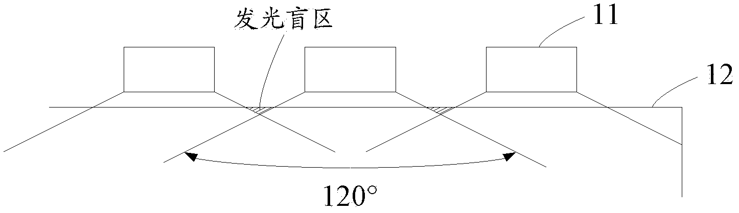
A liquid crystal display device, LED packaging technology, applied in the direction of instruments, electrical components, circuits, etc., can solve the problems of poor light mixing, small viewing angle range of LED lamps, and reduced light utilization rate, so as to eliminate the HotSpot phenomenon and avoid luminescence. Blind area, the effect of increasing the mixing distance

Active Publication Date: 2012-06-27
SHENZHEN CHINA STAR OPTOELECTRONICS TECH CO LTD
View PDF7 Cites 0 Cited by
  • Summary
  • Abstract
  • Description
  • Claims
  • Application Information

AI Technical Summary

Problems solved by technology

like figure 1 As shown, the viewing angle range of the elliptical LED lamp 11 is 120°. When the LED lamps 11 are arranged in a straight line on the light guide plate 12, there is a lighting blind area between two adjacent LED lamps 11 due to the limitation of the viewing angle range.
If the light incident surface of the light guide plate 12 is very close to the LED lamp 11, no light will pass through the light guide plate 12 located in the blind area, and the corresponding area of ​​the blind area will be relatively dark, while other areas irradiated by the LED lamp 11 will be brighter. There is an obvious alternation of light and dark, which in turn leads to the phenomenon of light and dark separation (Hot Spot) at the light entrance of the liquid crystal display device, resulting in poor light mixing
If the distance between the light guide plate 12 and the LED lamp 11 is increased, although the Hot Spot problem can be eliminated, the viewing angle range of the LED lamp 11 is reduced, so that the utilization rate of light decreases

Method used


Image

  • Liquid-crystal display device and LED (Light-Emitting Diode) packaging structure thereof
  • Liquid-crystal display device and LED (Light-Emitting Diode) packaging structure thereof
  • Liquid-crystal display device and LED (Light-Emitting Diode) packaging structure thereof

Examples


Embodiment Construction

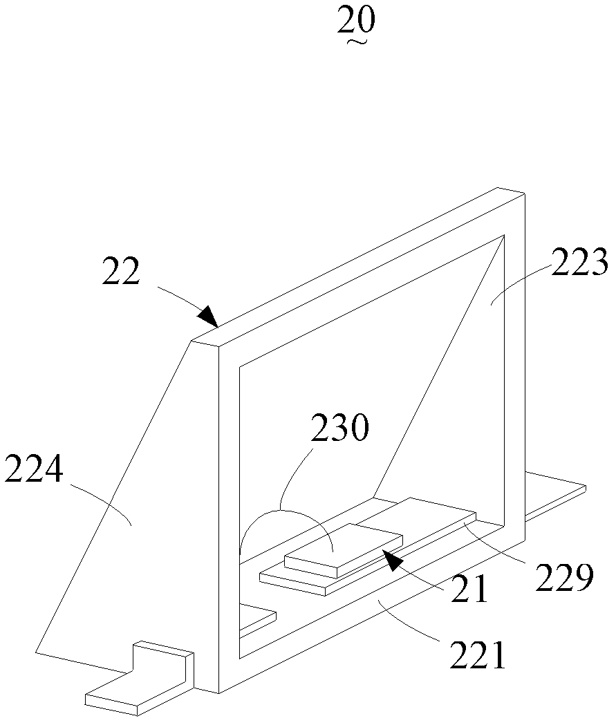
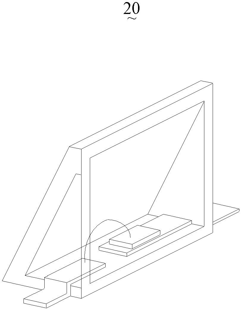
[0027] See Figure 2-4 , figure 2 is a schematic perspective view of the LED packaging structure according to the first embodiment of the present invention, image 3 yes figure 2 The perspective view of the LED package structure in, Figure 4 yes figure 2 A schematic cross-sectional view of the LED package structure in Fig. Such as Figure 2-4 As shown, the LED packaging structure 20 of this embodiment includes: an LED chip 21 and a frame 22 for accommodating the LED chip 21 . Wherein, the frame body 22 includes a bottom wall 221 , a first side wall 222 , a second side wall 223 , a third side wall 224 and a light-emitting wall 225 . The LED package structure 20 also includes solder pins 229 and wires 230 .

[0028] In this embodiment, the soldering legs 229 are arranged on the bottom wall 221 and include a first part of the soldering legs and a second part of the soldering legs. . That is, the LED chip 21 is disposed on the bottom wall 221 , and the first side wall...


PUM


Abstract

The invention provides an LED (Light-Emitting Diode) packaging structure, which comprises an LED chip and a frame body, wherein the frame body is used for containing the LED chip, the frame body comprises a bottom wall, a first lateral wall and a light-emitting wall, the LED chip is arranged on the bottom wall, the first lateral wall is obliquely arranged on the light-emitting direction of the LED chip, and rays emitted by the LED chip are emitted out of the light-emitting wall after being reflected through the first lateral wall. The invention further provides a liquid-crystal display device. In the mode, the rays emitted by the liquid-crystal display device and the LED chip in the LED packaging structure of the liquid-crystal display device disclosed by the invention are emitted out of the light-emitting wall after being reflected through the first lateral wall, so that the light-mixing distance of the LED chip is further increased, the generation of a light-emitting blind area is avoided, and the phenomenon of hot spots can be eliminated.

Description

technical field [0001] The invention relates to the field of display technology, in particular to a liquid crystal display device and an LED packaging structure thereof. Background technique [0002] At present, the application of liquid crystal display devices is becoming more and more popular. In the prior art, liquid crystal display devices include a backlight module. The backlight module includes a light source module and a light guide plate. The light source module is arranged on the light incident surface of the light guide plate. Light Emitting Diode (LED). All LED lights have a certain range of viewing angles, such as oval LED lights. Such as figure 1 As shown, the viewing angle range of the elliptical LED lamp 11 is 120°. When the LED lamps 11 are arranged in a straight line on the light guide plate 12, there is a blind spot between two adjacent LED lamps 11 due to the limitation of the viewing angle range. If the light incident surface of the light guide plate 1...

Claims


Application Information

Patent Timeline
Patent Type & Authority Applications(China)
IPC IPC(8): H01L33/60H01L33/48G02F1/13357
CPCH01L33/54H01L33/58H01L33/486G02F1/133615H01L2224/48091G02B6/0001H01L33/60H01L2224/48247G02B6/0031G02B6/0073H01L2924/00014
Inventor 唐国富俞刚
Owner SHENZHEN CHINA STAR OPTOELECTRONICS TECH CO LTD
Why Eureka
Try Eureka