Method for manufacture of multi-layer-multi-turn high efficiency inductors with cavity

a manufacturing method and high efficiency technology, applied in the direction of loop antennas, near-field read/write/interrogation/identification systems, magnets, etc., to achieve the effect of increasing the conductance area of the inductor structure, reducing quality factors, and increasing resistive losses

Active Publication Date: 2013-08-15
NUCURRENT INC
View PDF5 Cites 84 Cited by
  • Summary
  • Abstract
  • Description
  • Claims
  • Application Information

AI Technical Summary

Benefits of technology

[0018]The teachings herein alleviate one or more of the above noted problems of higher resistive losses at high frequencies resulting in lower quality factors by utilizing the multi-layer wire concept to increase the area of conductance within an inductor structure. The multi-layer wire configuration results in a reduction of resistance loss and an increase in the qualify factor of the inductor structure and resulting electrical circuit. The present teachings apply to the structure and design of a novel inductor for incorporation within electrical circuits. Most notably electrical circuits that operate within and above the radio frequency range of at least 3 kHz.
[0019]One aspect of the present teachings is of an inductor wherein resistive losses within the inductor are minimized by maximizing useful conductor cross-sectional area in a wire cross section. In one embodiment, the inductor mitigates the unwanted high frequency skin effect by creating the following structure: by introducing non-conducting or poorly conductive dielectric layers within its wire, resulting in a structure that comprises layers of conducting material alternating with layers of non-conducting or poorly conducting material. The structure effectively provides an increased number of surfaces each with its characteristic skin depth and all electrically, or otherwise, connected. The skin depth may range from approximately one-half of the conductor depth to about equal to the conductor depth. The conductor depth may be in the range of skin depth to twice the skin depth. However, depending on the available technology, costs, and application, the conductor depth may be as large as twenty times or more the skin depth.

Problems solved by technology

However, depending on the available technology, costs, and application, the conductor depth may be as large as twenty times or more the skin depth.

Method used


Image

  • Method for manufacture of multi-layer-multi-turn high efficiency inductors with cavity
  • Method for manufacture of multi-layer-multi-turn high efficiency inductors with cavity
  • Method for manufacture of multi-layer-multi-turn high efficiency inductors with cavity

Examples


examples

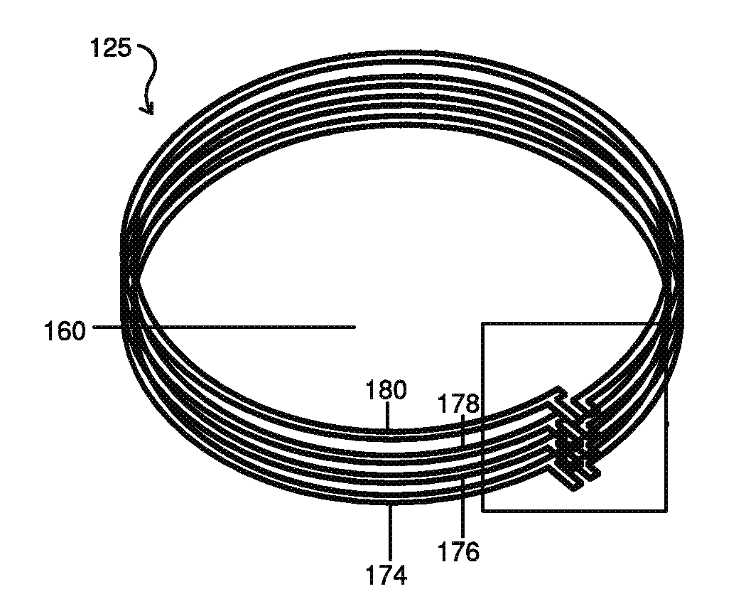
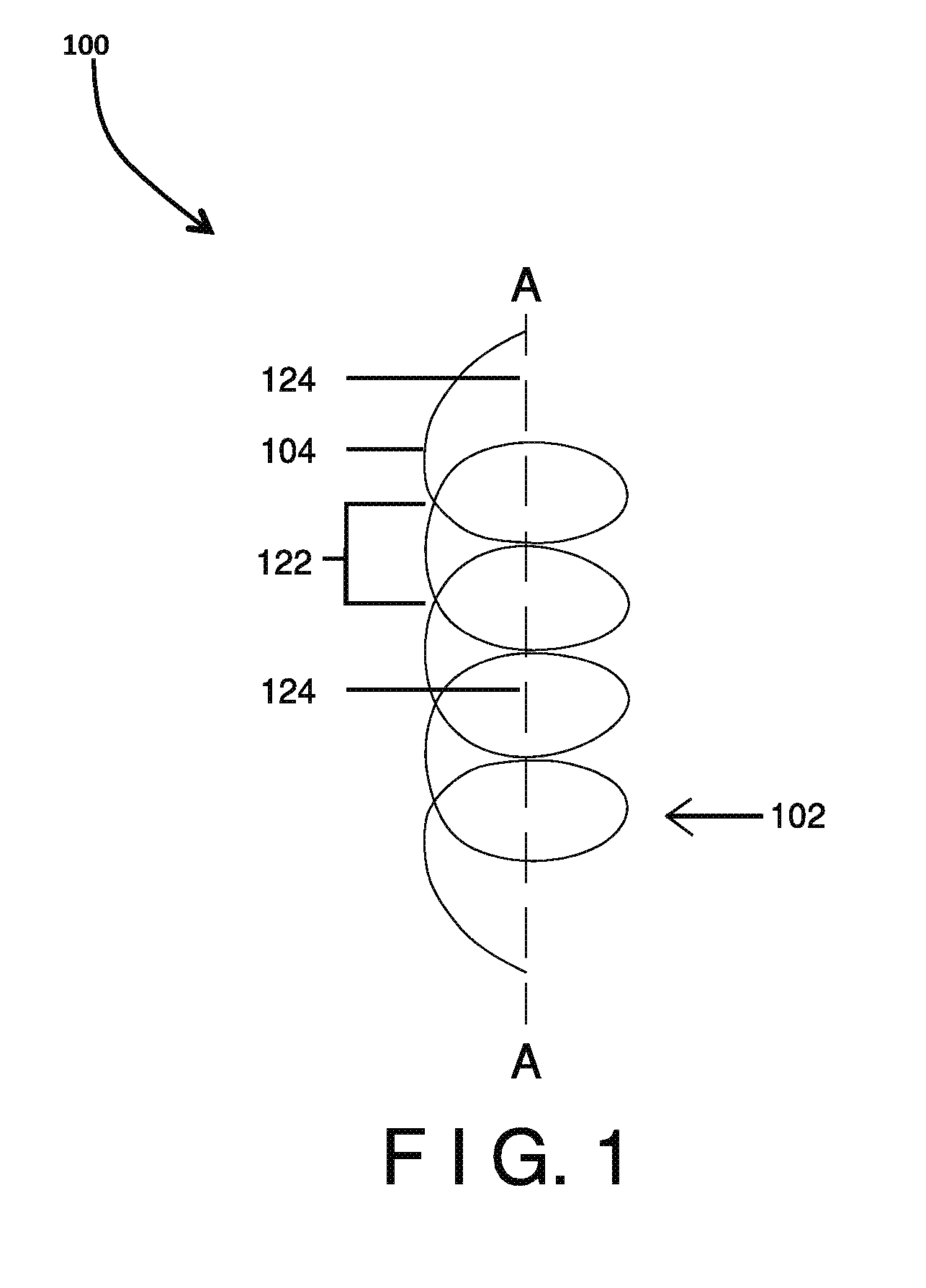
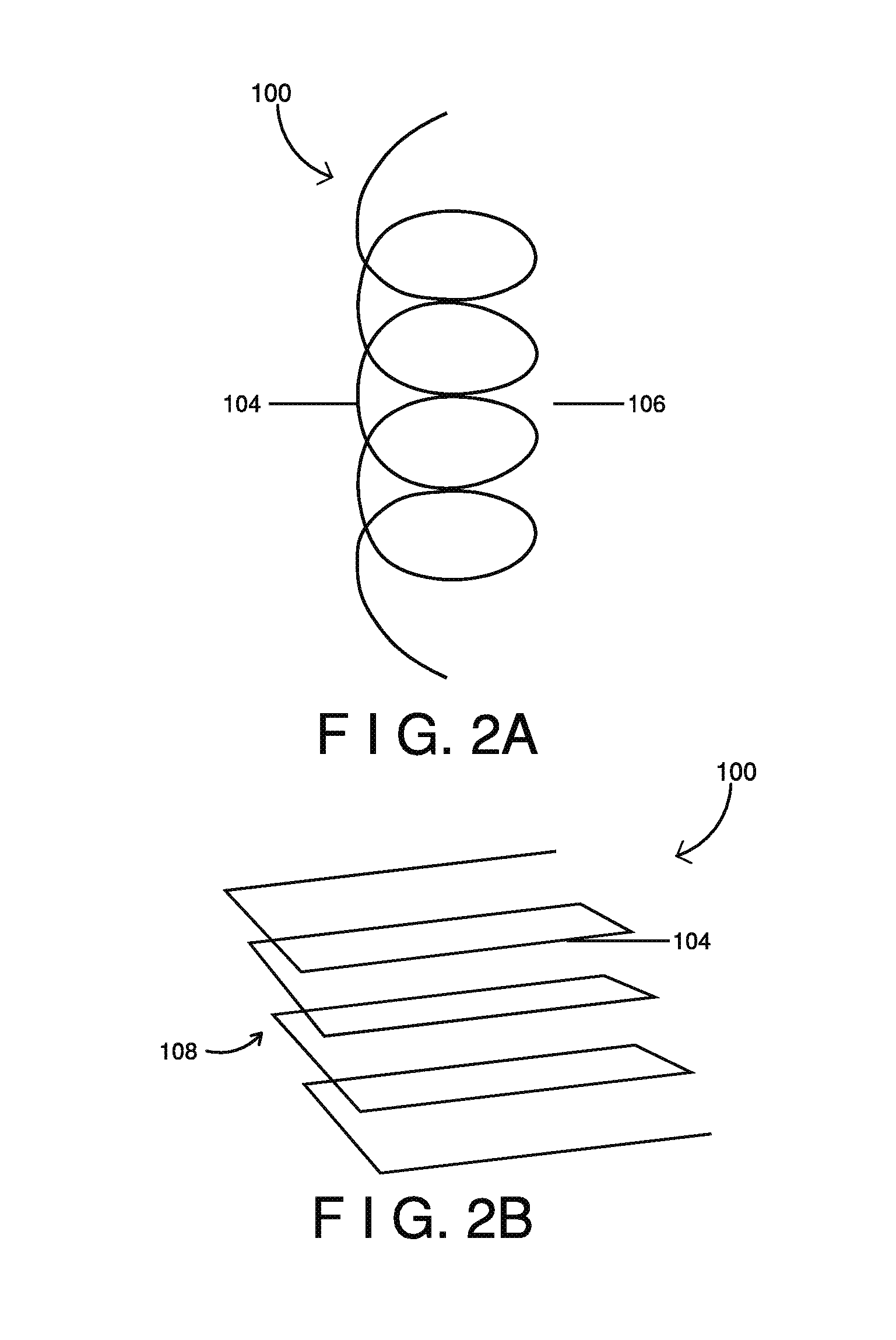
[0158]Table 1 illustrates an example wherein a TDK model MLG1608B4N7ST inductor was compared to a computer generated model of an MLMT inductor 125 of the present invention. The MLMT inductor 125 modeled such that it provides an inductance that is similar to the TDK model inductor. As shown in Table 1 below, the MLMT inductor of the present invention has a similar inductance of about 4.72 nH vs. the 4.7 nH of the TDK inductor operating at 100 MHz. However, the quality factor of the MLMT inductor 125 was determined to be about 2.8 times greater than the TDK inductor operating at about 100 MHz.

TABLE 1TDKMLMT InductorInductanceInductanceFrequency(nH)Quality Factor(nH)Quality Factor100 MHz4.7104.7238

[0159]Table 2 illustrates an example wherein a Sunlord model HQ1005C1N5 inductor was compared to a computer generated model of an MLMT inductor 125 of the present invention. The MLMT inductor 125 was modeled to provide an inductance that is similar to the Sunlord model inductor. As shown in T...


PUM

PropertyMeasurementUnit
thicknessaaaaaaaaaa
inductanceaaaaaaaaaa
operating frequenciesaaaaaaaaaa

Abstract

A multi-layer, multi-turn structure for an inductor having a plurality of conductor layers separated by layers of insulator is described. The inductor further comprises a connector electrically connected between the conductor layers. The structure of the inductor may comprise a cavity therewithin. The structure of the inductor constructed such that electrical resistance is reduced therewithin, thus increasing the efficiency of the inductor. The inductor is particularly useful at operating within the radio frequency range and greater.

Description

CROSS-REFERENCE TO RELATED APPLICATIONS[0001]The present application is a continuation-in-part of U.S. application Ser. No. 13 / 233,569, filed Sep. 15, 2011, which is a continuation-in-part of U.S. application Ser. No. 13 / 255,659, filed Sep. 9, 2011, which is a 371 application of International Application No. PCT / US2010 / 000714, filed Mar. 9, 2010, which is a nonprovisional of U.S. Provisional Application No. 61 / 158,688, filed Mar. 9, 2009, the disclosures of which are entirely incorporated herein by reference.[0002]The present application is a continuation-in-part of U.S. application Ser. No. 13 / 255,659, filed Sep. 9, 2011, which is a 371 application of International Application No. PCT / US2010 / 000714, filed Mar. 9, 2010, which is a nonprovisional of U.S. Provisional Application No. 61 / 158,688, filed Mar. 9, 2009, the disclosures of which are entirely incorporated herein by reference.[0003]The present patent application also hereby incorporates by reference the entire contents of U.S....

Claims


Application Information

Patent Timeline
Patent Type & Authority Applications(United States)
IPC IPC(8): H01F41/00
CPCH01F29/02H01F38/14H01F2027/2809H05K2201/0352H05K1/165H04B5/0075H04B5/0037H01F41/041H04B5/0031H01F41/00Y10T29/4902A61N1/0553A61N1/37229A61N1/3756A61N1/3787A61N1/3605H01F17/0013H04B5/0062H04B5/0068H01F27/2804H05B6/06H05B6/36H05B6/362H01F5/00H01F17/00H01F17/0006H01F41/04H05B6/1245Y10T29/49195Y10T29/49005Y10T29/4908Y10T29/49117Y10T29/49155H02J50/12H01F5/003H01Q7/00H02J50/005Y02B40/00H02J2310/23H01R43/00H01F7/06B33Y80/00H02P13/00H03H7/01H01Q1/38
Inventor SINGH, VINITBABCOCK, JACOBFRYSZ, CHRISTINE A.
Owner NUCURRENT INC
Why Eureka
Try Eureka