
Mosfet with work function adjusted metal backgate

a metal backgate and work function technology, applied in the field of metal oxide semiconductor field effect transistors, can solve the problems of increasing the complexity of the fabrication process and increasing the chip area, and achieve the effects of improving the backgate series resistance, reducing gate induced drain leakage, and reducing gidl and drain induced barrier leakag

Active Publication Date: 2013-08-22
GLOBALFOUNDRIES US INC
View PDF9 Cites 36 Cited by
  • Summary
  • Abstract
  • Description
  • Claims
  • Application Information

AI Technical Summary

Benefits of technology

[0015]An advantage of the present invention is that a backgate formed underneath the buried oxide is useful to control the device threshold voltage (herein “Vt”). By controlling the device threshold voltage multiple Vt devices can be achieved, device Vt can be controlled, or device power management can be controlled.
[0016]Another advantage of the present invention over other techniques is improved backgate series resistance afforded by use of a metal backgate rather than a doped silicon layer.
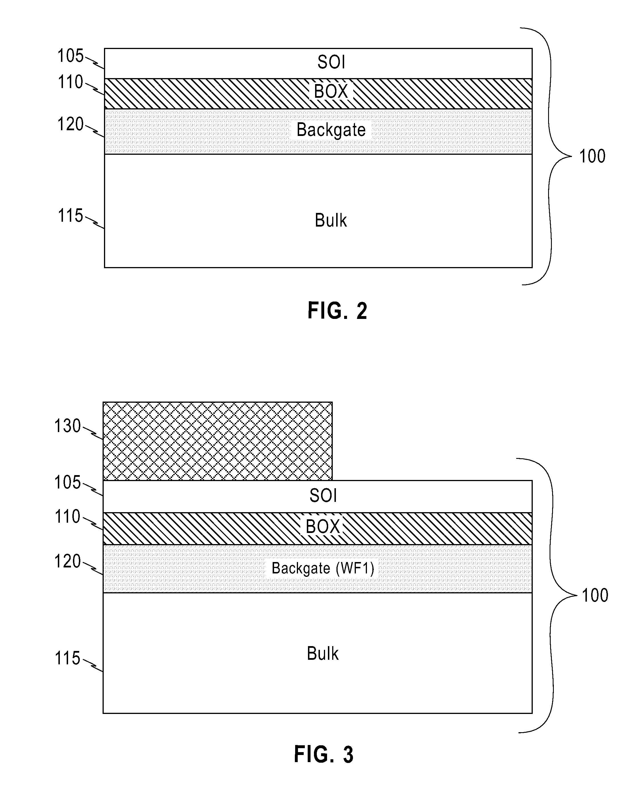
[0017]A further advantage of the present invention is that a work function tuning ion implantation can adjust the backgate work function for different portions of the wafer, for example under different field effect transistors.
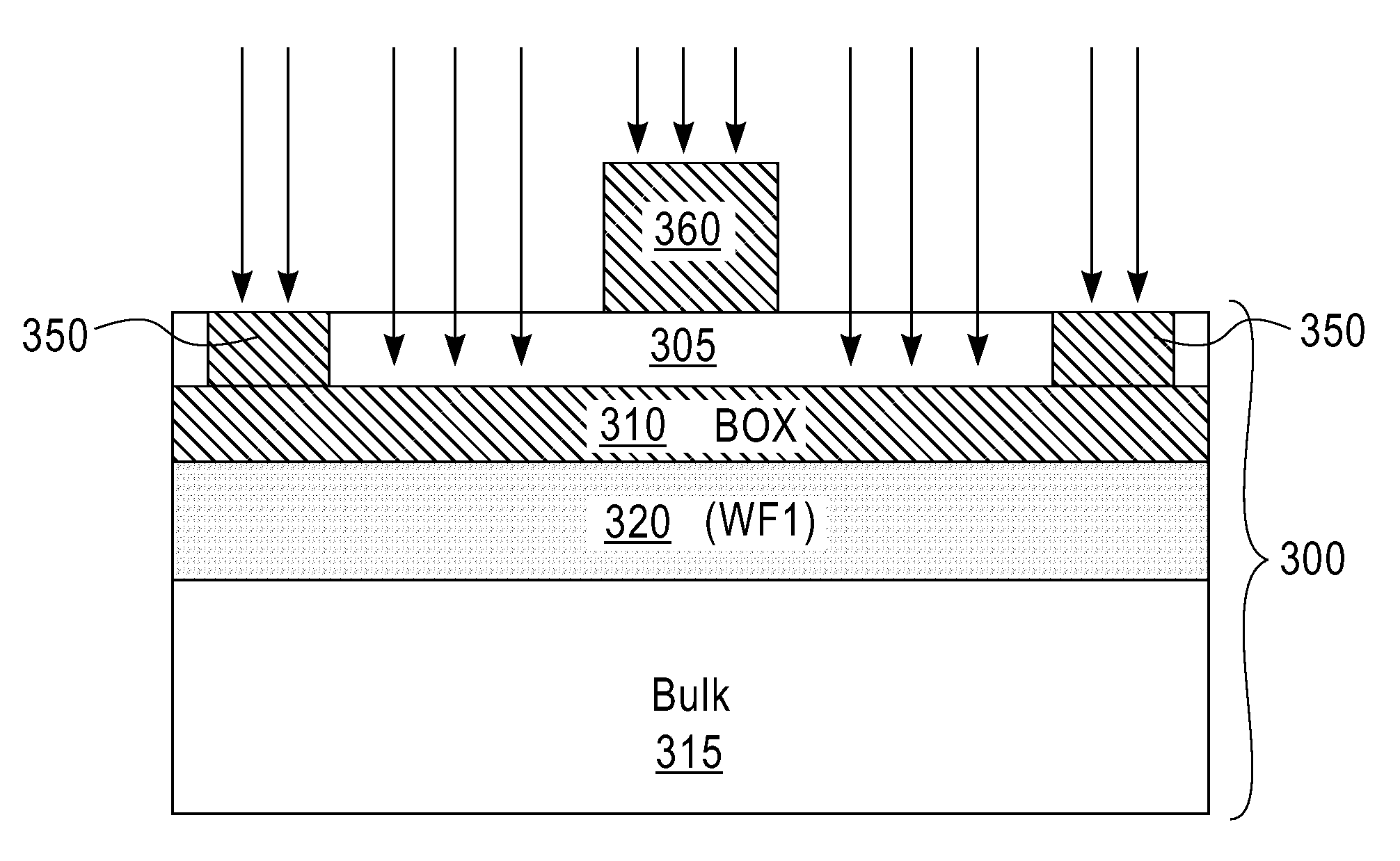
[0018]Yet another advantage of the present invention is that the work function tuning implant can be done during device processing (as opposed to substrate fabrication) so that the backgate work function underneath the channel region of a FET is different from the work function underneath the source / drain regions of the same FET. Such tuning can reduce Gate Induced Drain Leakage (herein “GIDL”)
[0019]An additional advantage is that the work function tuning implant can be tilted so that the backgate work function is different on the two sides of the a device. Such tuning can reduce GIDL and Drain Induced Barrier Leakage (herein “DIBL”).
[0020]Other characteristics and advantages of the invention will become obvious in combination with the description of accompanying drawings, wherein the same number represents the same or similar parts in all figures.

Problems solved by technology

The need for additional contacts, isolation areas, and circuits increases the complexity of the fabrication process and increased chip area.

Method used


Image

  • Mosfet with work function adjusted metal backgate
  • Mosfet with work function adjusted metal backgate
  • Mosfet with work function adjusted metal backgate

Examples


Embodiment Construction

[0052]The basic principle of the invention is a method of tuning work functions of MOSFET metal backgates by ion implantation. The method results in a structure which has at least two metal backgate work function regions. Work function tuning is a way to adjust threshold voltages of a device, thus creating two work function regions which, in turn creates two threshold voltage regions.

[0053]The methods to be described can be divided into two large categories: backgate work function tuning prior to device fabrication and backgate work function tuning during device fabrication.

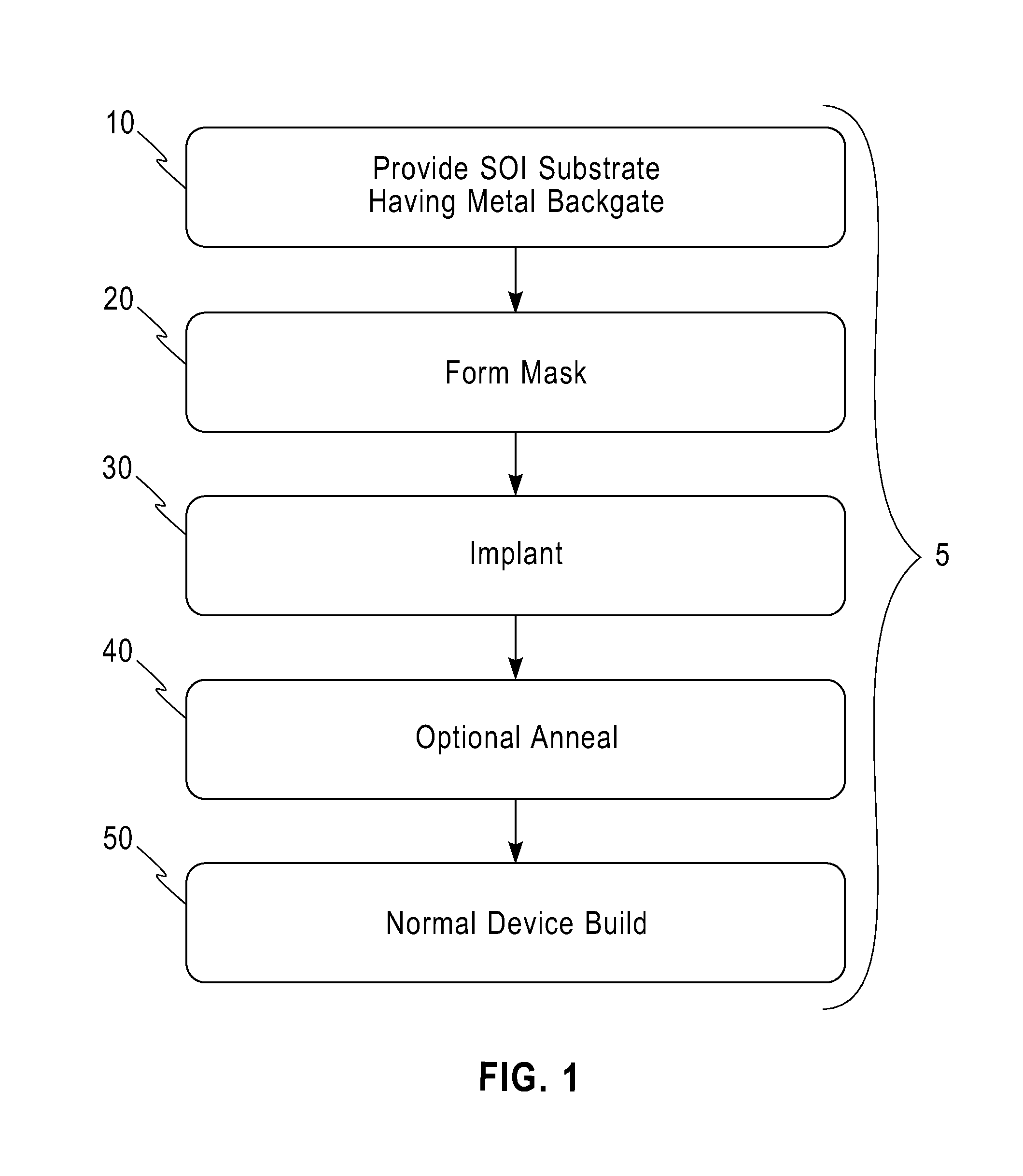
[0054]With respect to backgate work function tuning prior to device fabrication, an embodiment of a method and resulting structure will be described in conjunction with FIGS. 1-8. Here, tuning is done by implanting a masked substrate to create two regions in the metal backgate. By tuning prior to device fabrication, a transistor may be made above each backgate region resulting in different devices having differen...


PUM

PropertyMeasurementUnit
thicknessaaaaaaaaaa
thicknessaaaaaaaaaa
thicknessaaaaaaaaaa

Abstract

An SOI substrate, a semiconductor device, and a method of backgate work function tuning. The substrate and the device have a plurality of metal backgate regions wherein at least two regions have different work functions. The method includes forming a mask on a substrate and implanting a metal backgate interposed between a buried oxide and bulk regions of the substrate thereby producing at least two metal backgate regions having different doses of impurity and different work functions. The work function regions can be aligned such that each transistor has different threshold voltage. When a top gate electrode serves as the mask, a metal backgate with a first work function under the channel region and a second work function under the source/drain regions is formed. The implant can be tilted to shift the work function regions relative to the mask.

Description

BACKGROUND OF THE INVENTION[0001]1. Field of the Invention[0002]The present invention generally relates to a Metal Oxide Semiconductor Field Effect Transistors (MOSFETs) made on semiconductor on insulator (SOI) substrates. In particular, the invention relates to MOSFETs with a work function adjusted metal backgate.[0003]2. Description of Related Art[0004]Work function is a material property defined as the energy needed to move an electron from the Fermi level to vacuum. The work function of a material is of interest in MOSFET applications because tuning the work function of a top gate electrode defines the threshold voltage of the MOSFET and influences the transistor performance.[0005]A top gate electrode comprises a gate dielectric and a gate conductor, usually a metal. To change the top gate work function at least the following approaches have been used: using different metals or metal alloys, adjusting metal thicknesses, manipulating metal composition, or manipulating the gate di...

Claims


Application Information

Patent Timeline
Patent Type & Authority Applications(United States)
IPC IPC(8): H01L27/088H01L21/265
CPCH01L21/84H01L27/1203H01L21/26586H01L29/78648H01L21/2652H01L29/66772H01L21/76267H01L29/45H01L29/7831
Inventor CHENG, KANGGUODORIS, BRUCEKHAKIFIROOZ, ALIKULKARNI, PRANITA
Owner GLOBALFOUNDRIES US INC
Learn More