Touch display panel

a technology of touch display panel and display panel, which is applied in the field of touch display panel, can solve problems such as deteriorating the visual quality of the touch display panel, and achieve the effect of improving the visual

Inactive Publication Date: 2013-09-12
WINTEK CHINA TECH LTD +1
View PDF17 Cites 26 Cited by
  • Summary
  • Abstract
  • Description
  • Claims
  • Application Information

AI Technical Summary

Benefits of technology

[0007]The present invention is further directed to a touch display panel with better visual effect.
[0022]Based on the description above, in the touch display panel of the present invention, by setting specific included angles between the edge directions of the pixels and the edge directions of the upper dielectric pattern disposed above the intersected sensing series, the interference between the dielectric patterns (i.e. upper dielectric patterns or bottom dielectric patterns) and the shielding pattern can be destroyed. The problems such as the inner structures are easily seen due to the shielding pattern of the pixels enlarged by the dielectric patterns (i.e. upper dielectric patterns or bottom dielectric patterns) are solved. Therefore, the touch display panel can have better visual effect.

Problems solved by technology

However, in the conventional touch display panels, users can easily see the inner structures such as pixels, etc., and this affects thereby deteriorating the visual quality of the touch display panels.
Therefore, the visual quality of the touch display panel is still one of the most importance issues that need to be improved.

Method used


Image

  • Touch display panel
  • Touch display panel
  • Touch display panel

Examples


first embodiment

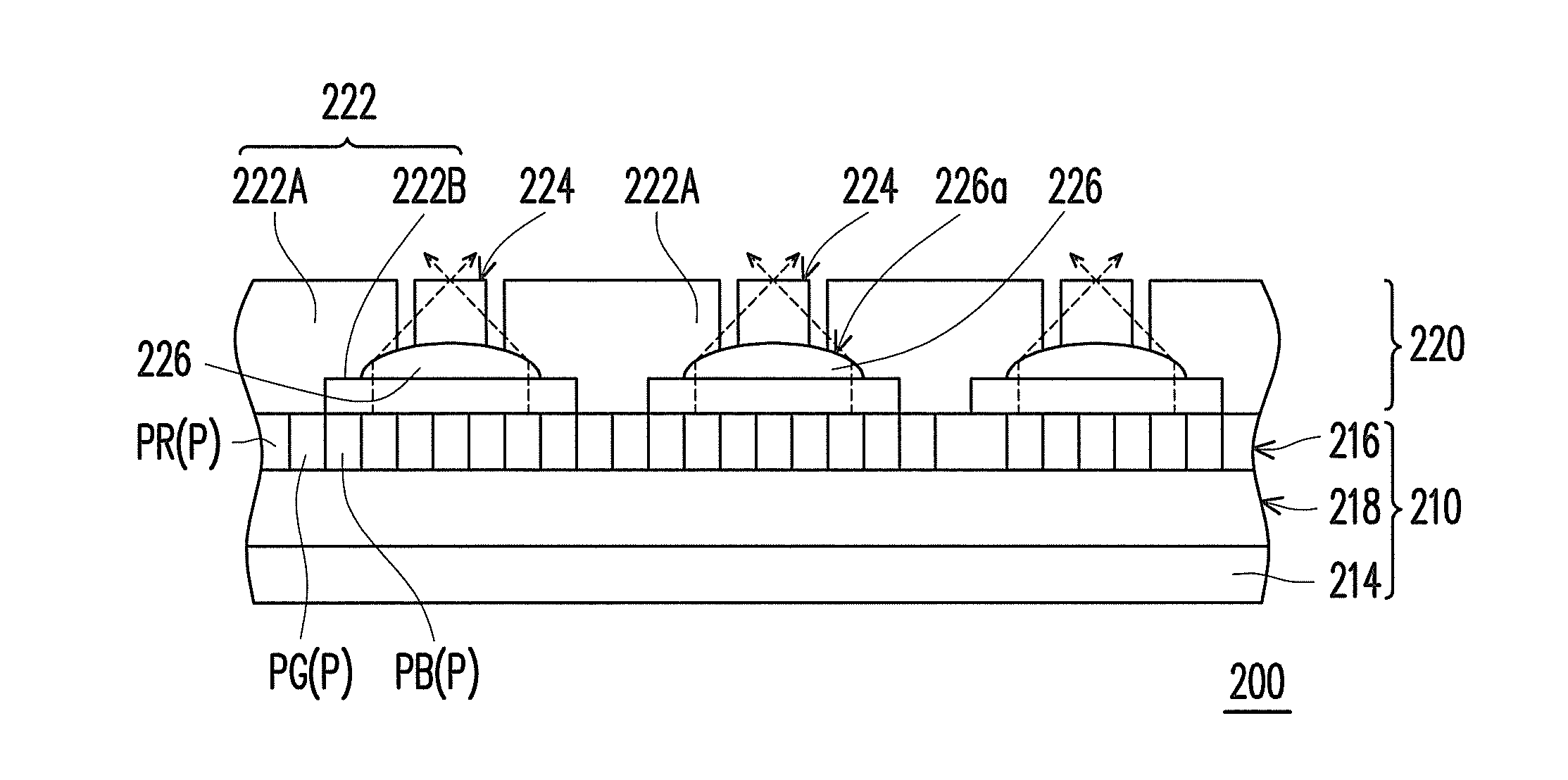
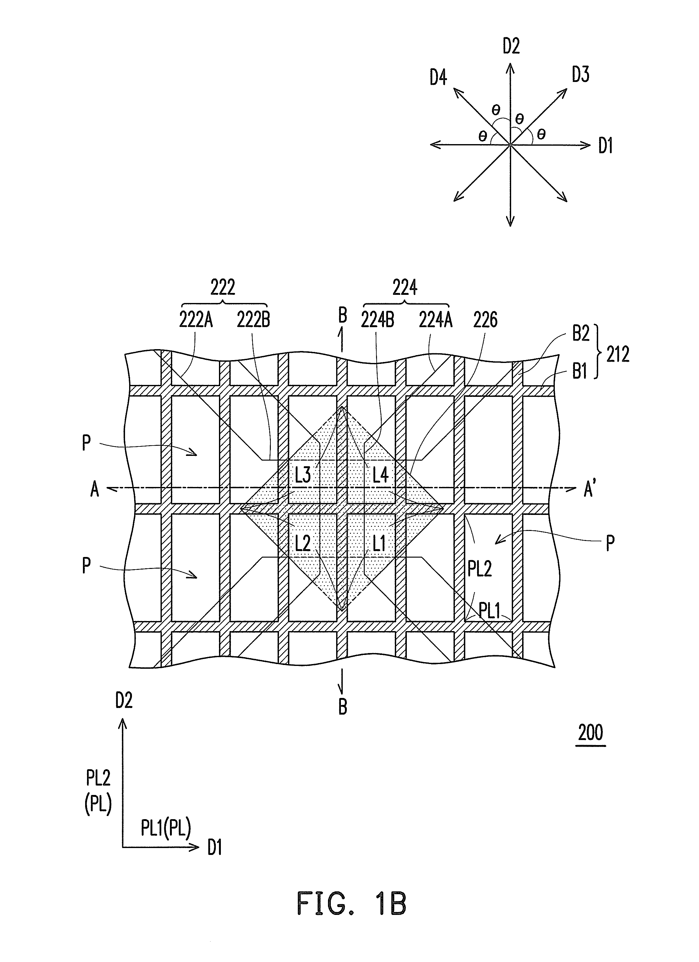
[0038]FIG. 1A is a schematic cross-sectional view of the touch display panel of one embodiment of the present invention. FIG. 1B is a schematic partial view of the arrangement of the pixels and the shielding pattern in the display panel and the arrangement of the sensing series and the dielectric patterns in the touch panel of FIG. 1A. FIG. 1A is a cross-sectional view taken along the section line A-A′ depicted in FIG. 1B. FIG. 1C is a cross-sectional view taken along the section line B-B′ depicted in FIG. 1B.

[0039]Please refer to both FIG. 1A and FIG. 1B, the touch display panel 200 includes a display panel 210 and a touch panel 220. The display panel 210 can be a LCD panel. In other embodiments, the display panel also may be an organic electro-luminescent display panel, an electrowetting display panel, or an electrophoretic display panel. The display panel 210 includes a shielding pattern 212 and a plurality of pixels P separated by the shielding pattern 212 wherein each pixel P c...

second embodiment

[0052]FIG. 5A is a schematic partial view of the arrangement of the pixels and the shielding pattern in the display panel and the arrangements of the sensing series and the dielectric patterns in the touch panel of second embodiment of the present invention. FIG. 5B is a cross-sectional view taken along the section line D-D′ depicted in FIG. 5A.

[0053]As shown in FIGS. 5A and 5B, in a touch display panel 300 of the present embodiment, the touch panel 320 is similar to touch panel 220 of the first embodiment in FIG. 1A-1C. The difference between touch panel 320 and touch panel 220 is that the touch panel 320 of the present embodiment further comprises upper dielectric pattern 336A.

[0054]More specifically, as shown in FIGS. 5A and 5B, the touch panel 320 includes a plurality of first sensing series 322, a plurality of second sensing series 324 and a plurality of upper dielectric patterns 326A. Each upper dielectric pattern 326A is disposed above an intersected region of each first sens...

third embodiment

[0057]FIG. 6 is a schematic cross-sectional view of the touch display panel of third embodiment of the present invention. As shown in FIG. 6, in a touch display panel 400 of the present embodiment, the touch panel 420 is similar to touch panel 320 of the second embodiment in FIG. 5A. The difference between touch panel 420 and touch panel 320 is that the size of upper dielectric pattern 426A of the present embodiment is greater than first connecting line 222B and second connecting line 224B. For clearer illustration, identical reference numerals are used on elements identical with those in the first embodiment.

[0058]More specifically, a projection of each upper dielectric pattern 426A of the present embodiment covers a projection of the corresponding first connecting line 222B or the corresponding second connecting line 224B onto the display panel 210. It should be noted that the contours can be blurred when the acute included angles between the edge directions of D3 and D4 of the re...


PUM


Abstract

A touch display panel including a display panel and a touch panel is provided. The display panel includes a shielding pattern and a plurality of pixels separated by the shielding pattern and including multiple edge directions. The touch panel is disposed on the display panel and includes a plurality of first sensing series, a plurality of second sensing series and a plurality of dielectric patterns. Each dielectric pattern is disposed between each first sensing series and each second sensing series intersected therewith, and includes multiple edge direction non-parallel to the edge direction of the pixel.

Description

CROSS-REFERENCE TO RELATED APPLICATION[0001]This application is a continuation-in-part of U.S. application Ser. No. 13 / 587,934, filed Aug. 17, 2012, all disclosure is incorporated therewith. The prior application Ser. No. 13 / 587,934 claims the priority benefit of Taiwan application serial no. 100129421, filed on Aug. 17, 2011. The entirety of each of the above-mentioned patent applications is hereby incorporated by reference herein and made a part of this specification.BACKGROUND OF THE INVENTION[0002]1. Field of the Invention[0003]The present invention generally relates to a touch display panel, and more particularly, to a touch display panel which can enhance the entire visual effect.[0004]2. Description of Related Art[0005]With the progress of electronic technology and the arrival of information era, many information products choose to use touch panels as the input device instead of the traditional input device such as keyboard, mouse, etc. The touch display panel with both touch...

Claims


Application Information

Patent Timeline
Patent Type & Authority Applications(United States)
IPC IPC(8): G06F3/041
CPCG06F3/0412G06F2203/04111G06F3/044
Inventor YEH, TA-WEIHSIEH, CHI-MINGCHOU, JEN-WEICHEN, CHIA-CHICHEN, HUI-CHUNYANG, HONG-EN
Owner WINTEK CHINA TECH LTD
Why Eureka
Try Eureka