Integrated circuit package having a split lead frame

a technology of integrated circuits and lead frames, which is applied in the direction of magnetic measurements, instruments, semiconductor devices, etc., can solve the problems of a large part of the overall cost of the sensor, the relatively expensive hard magnetic material used to form the magnet, and the high cost of the sensor

Active Publication Date: 2013-09-26
ALLEGRO MICROSYSTEMS INC
View PDF16 Cites 37 Cited by
  • Summary
  • Abstract
  • Description
  • Claims
  • Application Information

AI Technical Summary

Benefits of technology

[0018]Additional described features include one or more slots in the die attach portion of at least one of the plurality of leads, one or more widened portions of the connection portion of at least one of the plurality of leads, and a ferromagnetic mold material secured to a connection portion of at least one of t...

Problems solved by technology

While the use of a back bias magnet is advantageous in certain applications, the hard magnetic material used to form the magnet is relatively expensive and represents a significant part of the overall cost of...

Method used


Image

  • Integrated circuit package having a split lead frame
  • Integrated circuit package having a split lead frame
  • Integrated circuit package having a split lead frame

Examples


Embodiment Construction

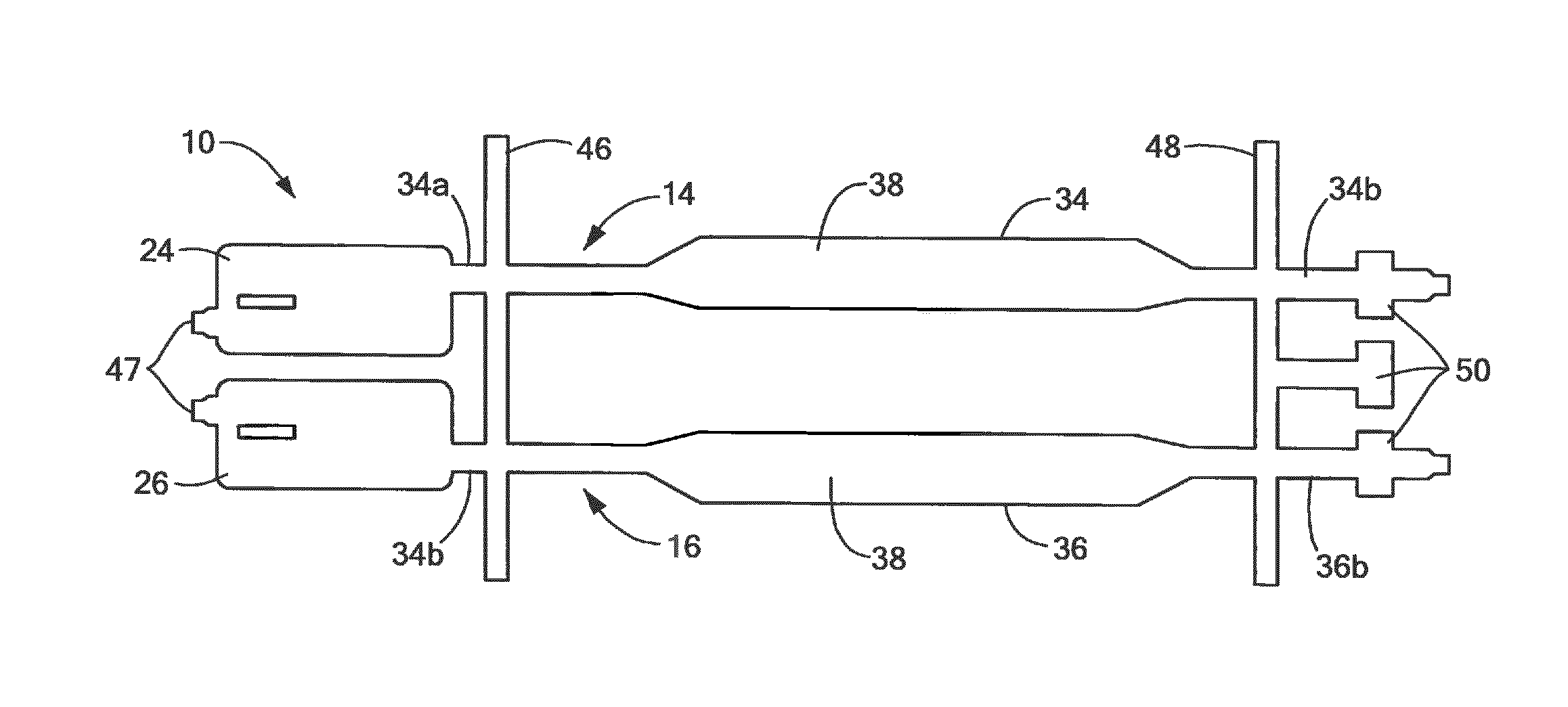
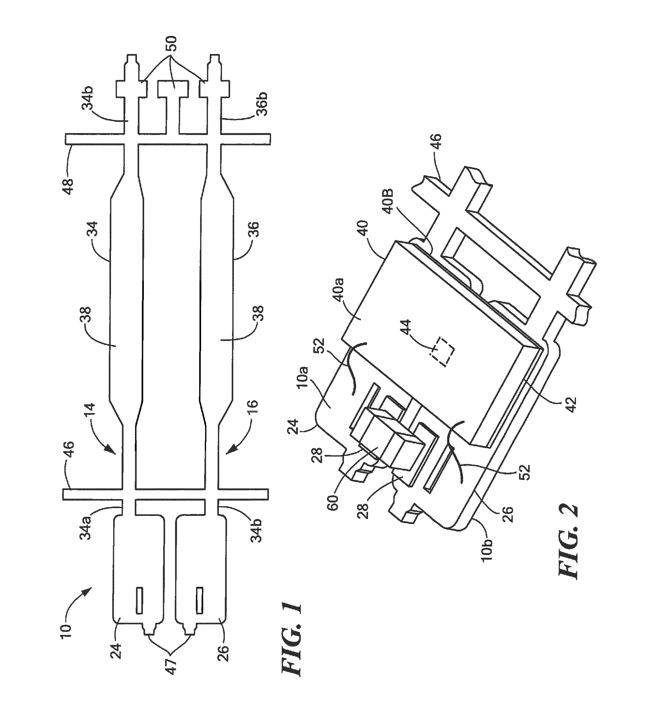
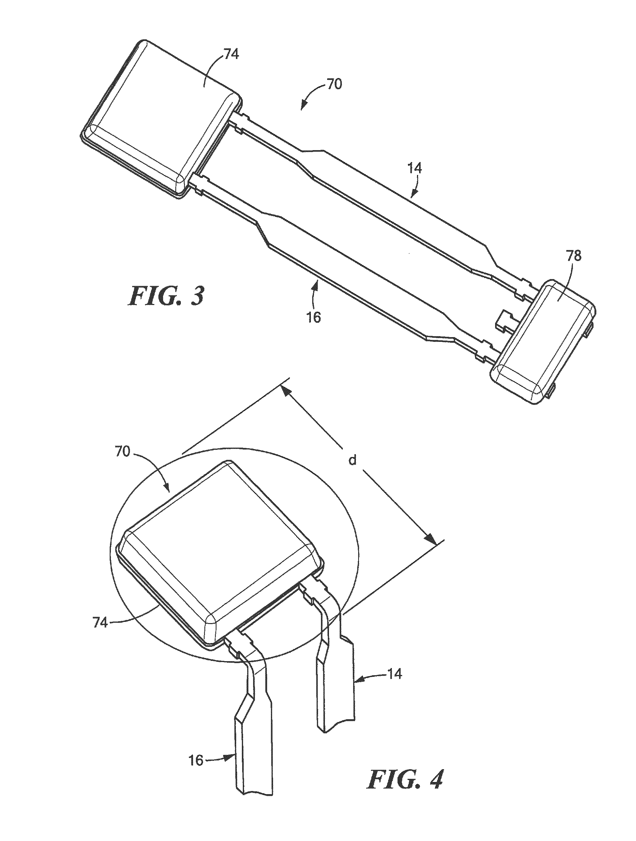
[0031]Referring to FIG. 1 a lead frame 10 for use in an integrated circuit includes a plurality of leads 14, 16, at least two of which (and here, the two illustrated leads comprising the plurality of leads) include a respective die attach portion 24, 26 and connection portion 34, 36. The lead frame 10 has a first surface 10a and a second, opposing surface 10b (FIG. 2). As will be explained, the die attach portion 24, 26 of the leads (referred to herein sometimes as simply the die portion) can have a semiconductor die (FIG. 2) attached thereto.

[0032]The connection portion 34, 36 of the leads extends from a first end 34a, 36a proximate to the respective die portion 24, 26 to a second, distal end 34b, 36b distal from the die portion. Generally, the connection portion 34, 36 of the leads is elongated and is suitable for making electrical connection to electronic systems and components (not shown) outside of the integrated circuit package, such as a power source or microcontroller. For e...


PUM


Abstract

A magnetic field sensor includes a lead frame having a plurality of leads, at least two of which have a connection portion and a die attach portion. A semiconductor die is attached to the die attach portion of the at least two leads. In some embodiments, at least one passive component is attached to the die attach portion of at least two leads.

Description

CROSS REFERENCE TO RELATED APPLICATIONS[0001]This application is a Continuation-in-Part application and claims the benefit of U.S. patent application Ser. No. 13 / 748,999, filed on Jan. 24, 2013, which is a Continuation-in-Part application and claims the benefit of U.S. patent application Ser. No. 13 / 424,618, filed on Mar. 20, 2012, both of which are incorporated herein by reference in their entirety.STATEMENT REGARDING FEDERALLY SPONSORED RESEARCH[0002]Not Applicable.FIELD OF THE INVENTION[0003]This invention relates generally to integrated circuit packaging and, more particularly, to an integrated circuit package having a split lead frame.BACKGROUND OF THE INVENTION[0004]Techniques for semiconductor packaging are well known in the art. In general, a semiconductor die is cut from a wafer, processed, and attached to a die attach pad of a lead frame. The subassembly may then be overmolded with a plastic or other insulative and protective material to form an integrated circuit (IC) pac...

Claims


Application Information

Patent Timeline
IPC IPC(8): G01R33/00
CPCG01R33/00G01R33/0011G01R33/0047H01L23/49562H01L23/49589H01L2224/32245H01L2224/73265H01L2224/48091H01L2224/48247H01L2924/00014H01L2224/16245H01L2224/48257H01L2924/00
Inventor DAVID, PAULTAYLOR, WILLIAM P.SCHELLER, P. KARLVIG, RAVIFRIEDRICH, ANDREAS P.
Owner ALLEGRO MICROSYSTEMS INC
Why Eureka
Try Eureka