Capacitive touch device and sensing method thereof

a capacitive touch and sensing device technology, applied in the direction of instruments, computing, electric digital data processing, etc., can solve the problems of affecting the overall structure, failing to meet the light and compact design,

Active Publication Date: 2013-10-03
NOVATEK MICROELECTRONICS CORP
View PDF0 Cites 13 Cited by
  • Summary
  • Abstract
  • Description
  • Claims
  • Application Information

AI Technical Summary

Benefits of technology

The invention relates to a technology that helps reduce interference when using a capacitive touch device by optimizing its sensing frequency based on real-life circumstances.

Problems solved by technology

The technical problem addressed in this patent relates to improving operational sensitivity of capacitive touch devices without adding excessive cost or changing their overall structure. This is because the performance of these devices depends on achieving a good signal-to-noise ratio (SNR), which requires effective measures to distinguish small variations in sensor results from noise sources like human static electricity, electronic equipment, etc.

Method used


Image

  • Capacitive touch device and sensing method thereof
  • Capacitive touch device and sensing method thereof
  • Capacitive touch device and sensing method thereof

Examples


Embodiment Construction

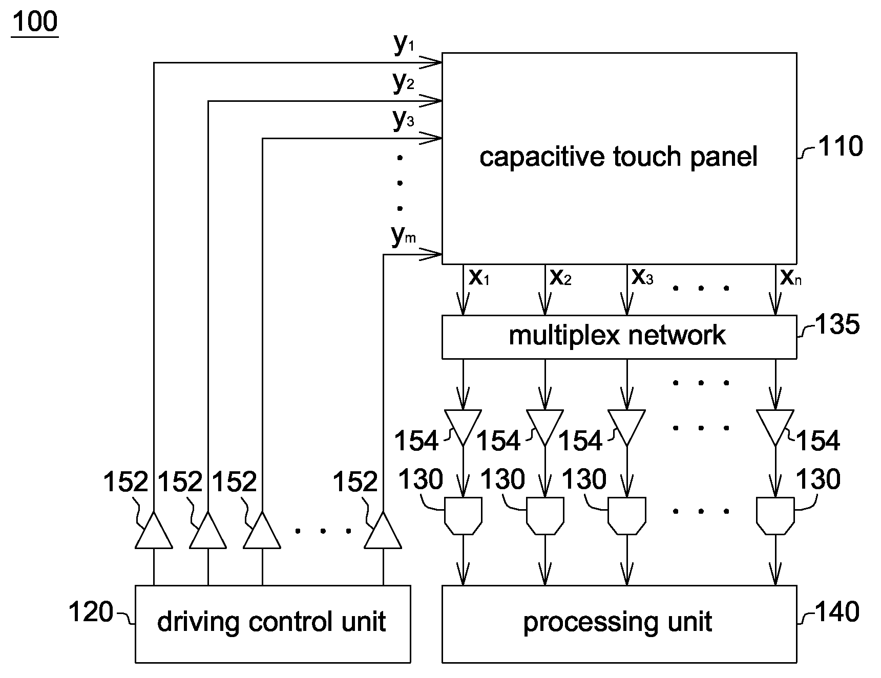
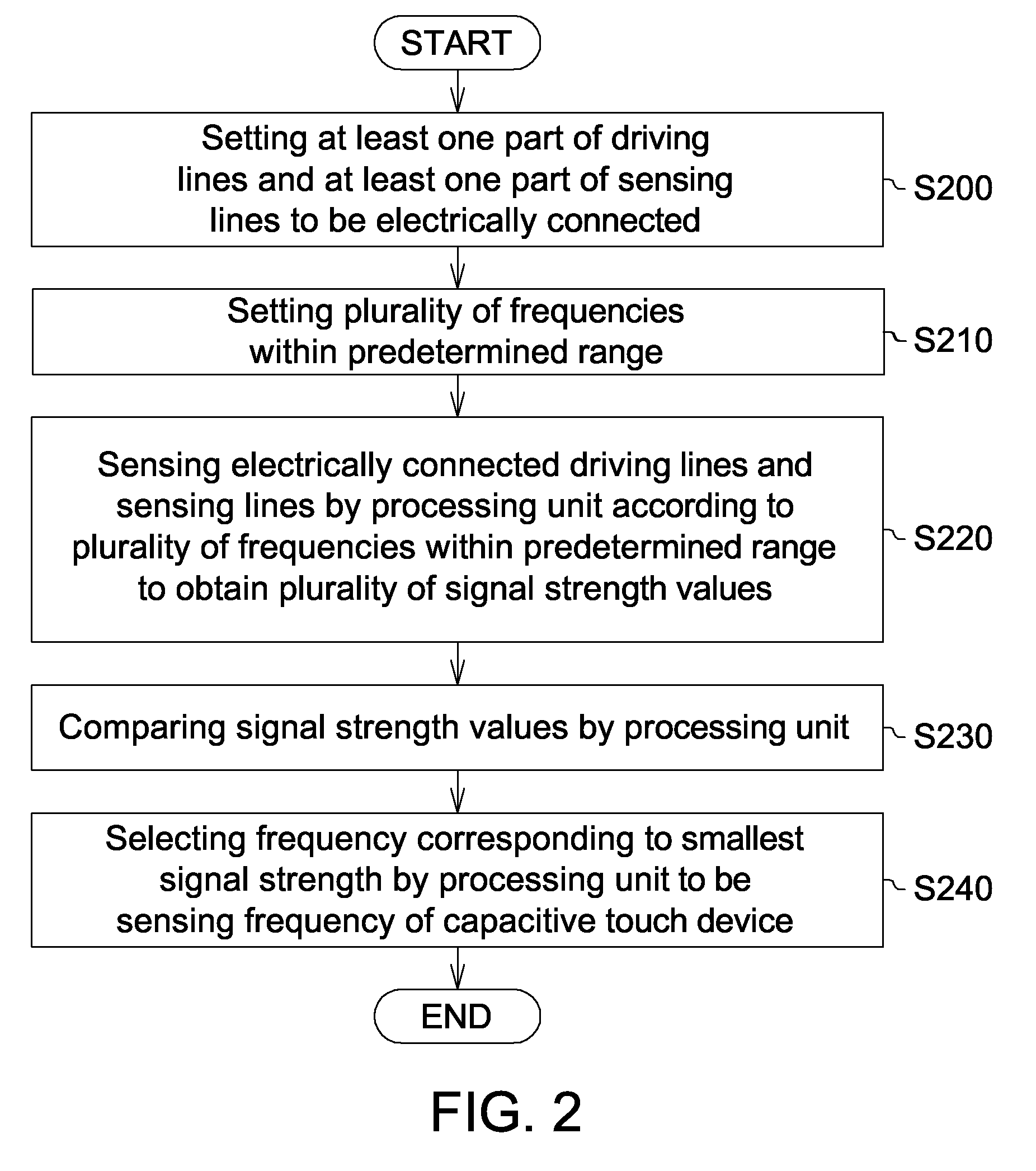
[0021]In a capacitive touch device and associate method provided by the disclosure, through connections between driving lines and sensing lines or a dummy scan line, an optimal sensing frequency is obtained according to sensed noise strengths to resist against noises in an actual operation environment.

[0022]FIG. 1 shows a block diagram of a capacitive touch device according to one embodiment. A capacitive touch device 100 includes a capacitive touch panel 110, a driving control unit 120, k analog-to-digital converters (ADCs) 130, a multiplex network 135 and a processing unit 140. The capacitive touch panel 110 has an m×n touch point matrix formed by m driving lines y1 to ym and n sensing lines x1 to xn, where m and n are a positive integer, respectively. The driving control unit 120 is coupled to the m driving lines y1 to ym. The capacitive touch device 100 may further include m amplifiers 152, and the driving control unit 120 may substantially be coupled to the m driving lines y1 t...


PUM


Abstract

A capacitive touch device includes a capacitive touch panel, a driving control unit, k ADCs, a multiplex network and a processing unit. The capacitive touch panel has an m×n sensing point matrix formed by m driving line and n sensing lines. The driving control unit is coupled to the m driving lines. The multiplex network connects the n sensing lines and the k ADCs by time-domain multiplexing. The processing unit is coupled to the k ADCs. At least a part of the driving lines and at least a part of the sensing lines are assigned to be electrically connected. The processing unit senses according to multiple frequencies to obtain multiple signal strength values, and selects the frequency corresponding to a smallest signal value to be a sensing frequency of the capacitive touch device.

Description


Claims


Application Information

Patent Timeline
Owner NOVATEK MICROELECTRONICS CORP
Why Eureka
Try Eureka