Method for manufacturing image sensor module

a manufacturing method and image sensor technology, applied in the direction of semiconductor/solid-state device testing/measurement, radio frequency controlled devices, instruments, etc., can solve the problems of increased manufacturing cost, noise in the obtained images, and further increase in manufacturing cost, so as to reduce thickness and volume, the effect of increasing manufacturing yield

Inactive Publication Date: 2013-11-21
SK HYNIX INC
View PDF4 Cites 1 Cited by
  • Summary
  • Abstract
  • Description
  • Claims
  • Application Information

AI Technical Summary

Benefits of technology

[0008]Embodiments of the present invention include an image sensor module which has a reduced thickness and volume, increased manufacturing yield, and which prevents unnecessary external light from being incident on image sensors and the resulting noise therefrom.

Problems solved by technology

When manufacturing image sensor modules glass substrates are inevitably disposed on defective semiconductor chips of a wafer as well as good semiconductor chips.
The packaging process is then conducted for not only the good but also the defective semiconductor chips causing increased manufacturing cost.
These spacers complicate the manufacturing process of an image sensor causing further increase in manufacturing cost.
However, in such a configuration light is likely to be incident on portions of the image sensor module aside from the image sensor leading to the presence of noise in the images obtained from the image sensors.

Method used


Image

  • Method for manufacturing image sensor module
  • Method for manufacturing image sensor module
  • Method for manufacturing image sensor module

Examples


Embodiment Construction

[0036]It is understood herein that the drawings are not necessarily to scale and in some instances proportions may have been exaggerated in order to more clearly depict certain features of the invention.

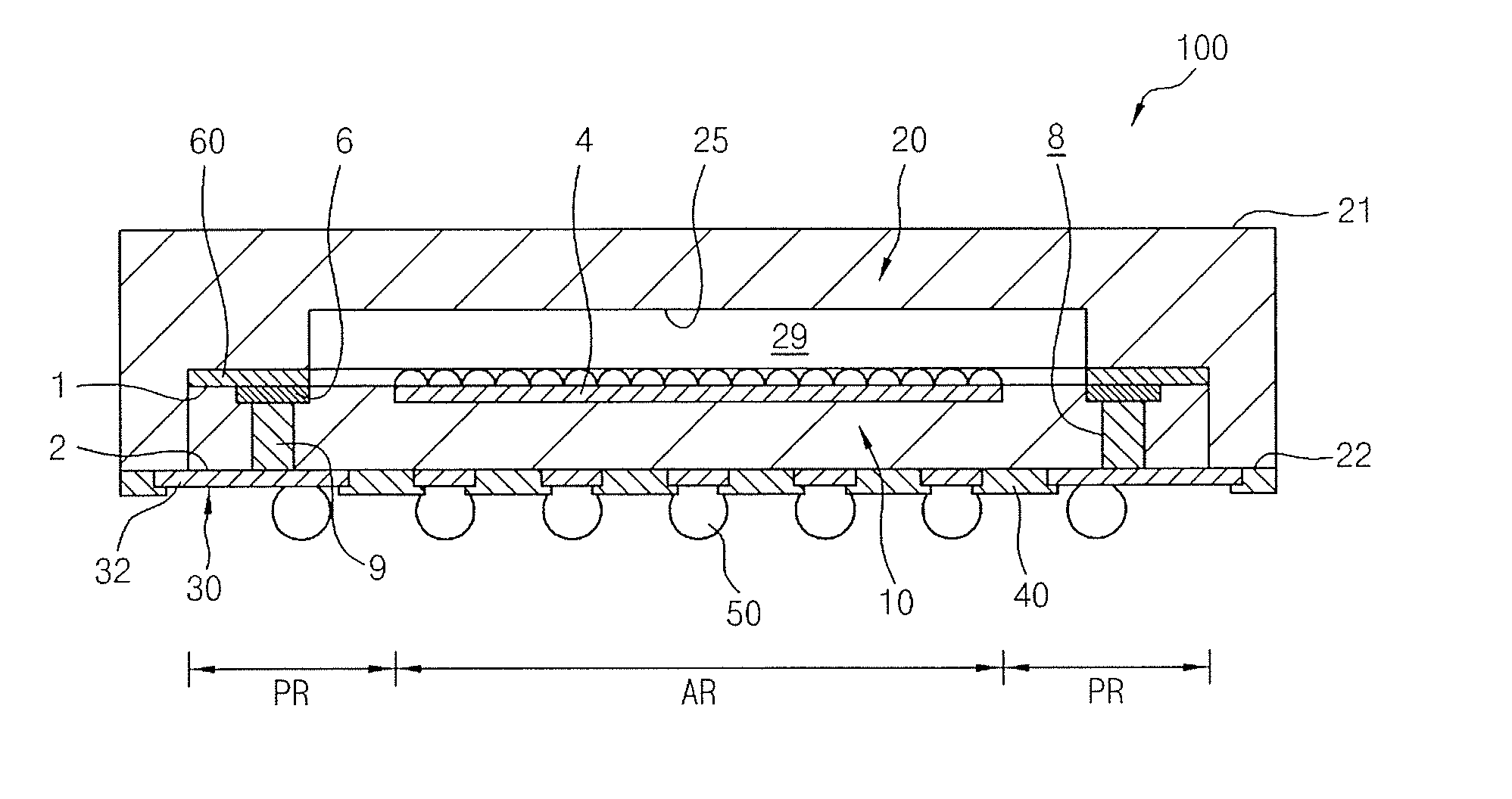
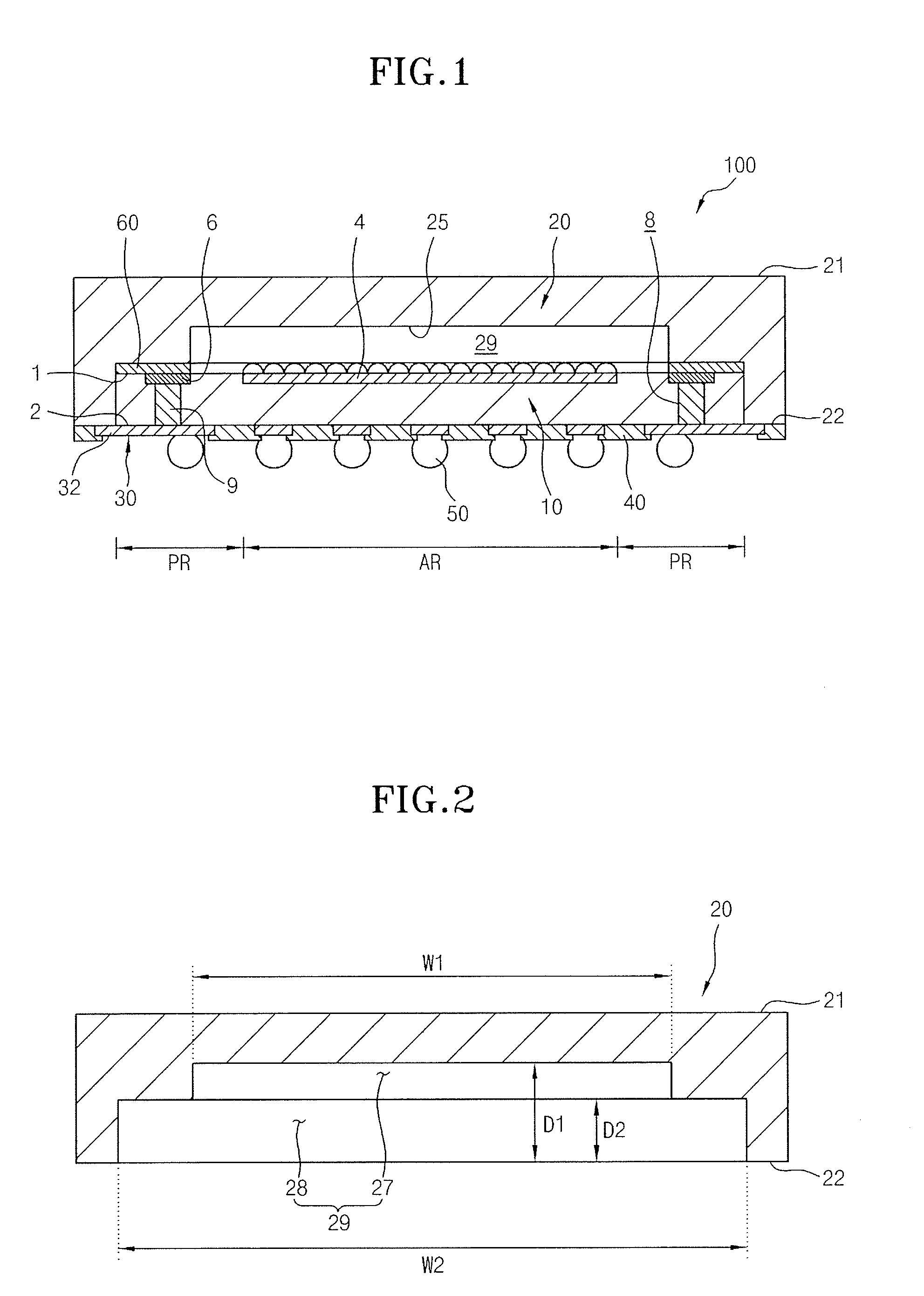
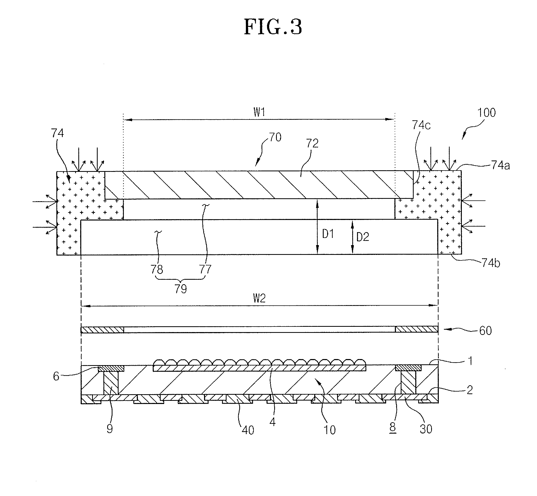
[0037]FIG. 1 is a cross-sectional view showing an image sensor module in accordance with an embodiment of the present invention.

[0038]Referring to FIG. 1, an image sensor module 100 includes a semiconductor chip 10, a transparent substrate 20, and metal lines 30.

[0039]In an embodiment, the semiconductor chip 10 has, for example, the shape of a plate with a small thickness. The semiconductor chip 10 has an upper surface 1 and a lower surface 2 facing away from the upper surface 1. An image sensor region AR is defined on the center portion of the semiconductor chip 10, and a peripheral region PR is defined in a band-like shape along the periphery of the image sensor region AR. In an embodiment, the image sensor region AR can have a quadrangular sectional shape when viewed from the top ...


PUM


Abstract

An image sensor module includes a semiconductor chip, a transparent substrate, and metal lines. The semiconductor chip includes image sensors disposed in an image sensor region, pads electrically connected to the image sensors and disposed in a peripheral region defined along a periphery of the image sensor region, and through-electrodes electrically connected to the pads. The transparent substrate has a groove defined by a surface covering the image sensors and the pads of the semiconductor chip. The metal lines are disposed on a lower surface of the semiconductor chip and are electrically connected to the through-electrodes.

Description

CROSS-REFERENCE TO RELATED APPLICATIONS[0001]The present application claims priority to Korean patent application number 10-2009-0073508 filed on Aug. 10, 2009, which is incorporated herein by reference in its entirety.BACKGROUND OF THE INVENTION[0002]The present invention relates to an image sensor module.[0003]In general, an image sensor module is defined as a device for converting light as an analog signal into an electrical signal.[0004]In developing an image sensor module it is desirable to obtain a high degree of resolution. A typical image sensor module is formed on a wafer and undergoes a packaging process. The image sensor includes semiconductor chips in which image sensors are formed, and glass substrates are disposed on the respective semiconductor chips.[0005]When manufacturing image sensor modules glass substrates are inevitably disposed on defective semiconductor chips of a wafer as well as good semiconductor chips. The packaging process is then conducted for not only ...

Claims


Application Information

Patent Timeline
Patent Type & Authority Applications(United States)
IPC IPC(8): H01L21/66
CPCH01L22/14H01L27/14618H01L27/14683H01L2924/01078H01L2924/01079H01L24/05H01L24/13H01L2224/02372H01L2224/05548H01L2224/05567H01L2224/13022H01L2224/13024H01L2924/00014H01L2924/0002H01L2224/0401H01L2924/12042H04N23/54H01L2224/05552H01L2924/00H01L27/146
Inventor YANG, SEUNG TAEK
Owner SK HYNIX INC
Why Eureka
Try Eureka