
Photosensitive imaging devices and associated methods

a technology of imaging devices and associated methods, applied in the direction of radiation control devices, semiconductor devices, electrical equipment, etc., can solve problems such as the problem of silicon-based technologies for detecting infrared incident electromagnetic radiation

Active Publication Date: 2014-07-17
SIONYX
View PDF8 Cites 52 Cited by
  • Summary
  • Abstract
  • Description
  • Claims
  • Application Information

AI Technical Summary

Benefits of technology

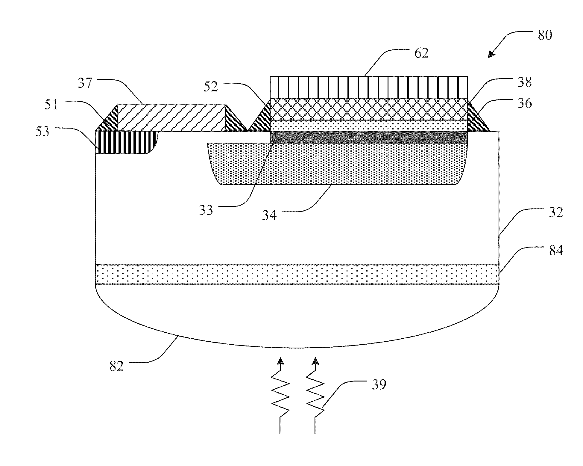
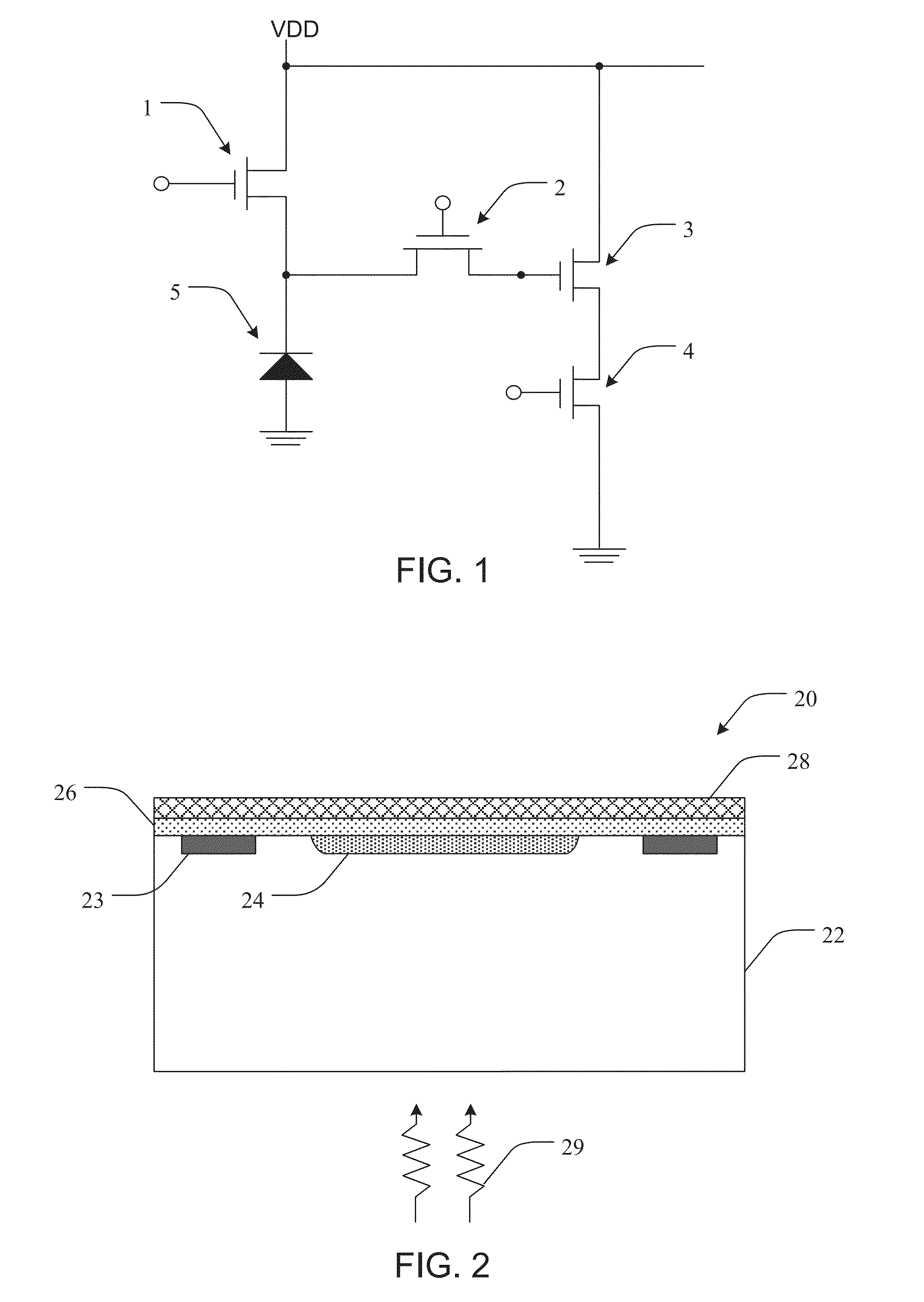
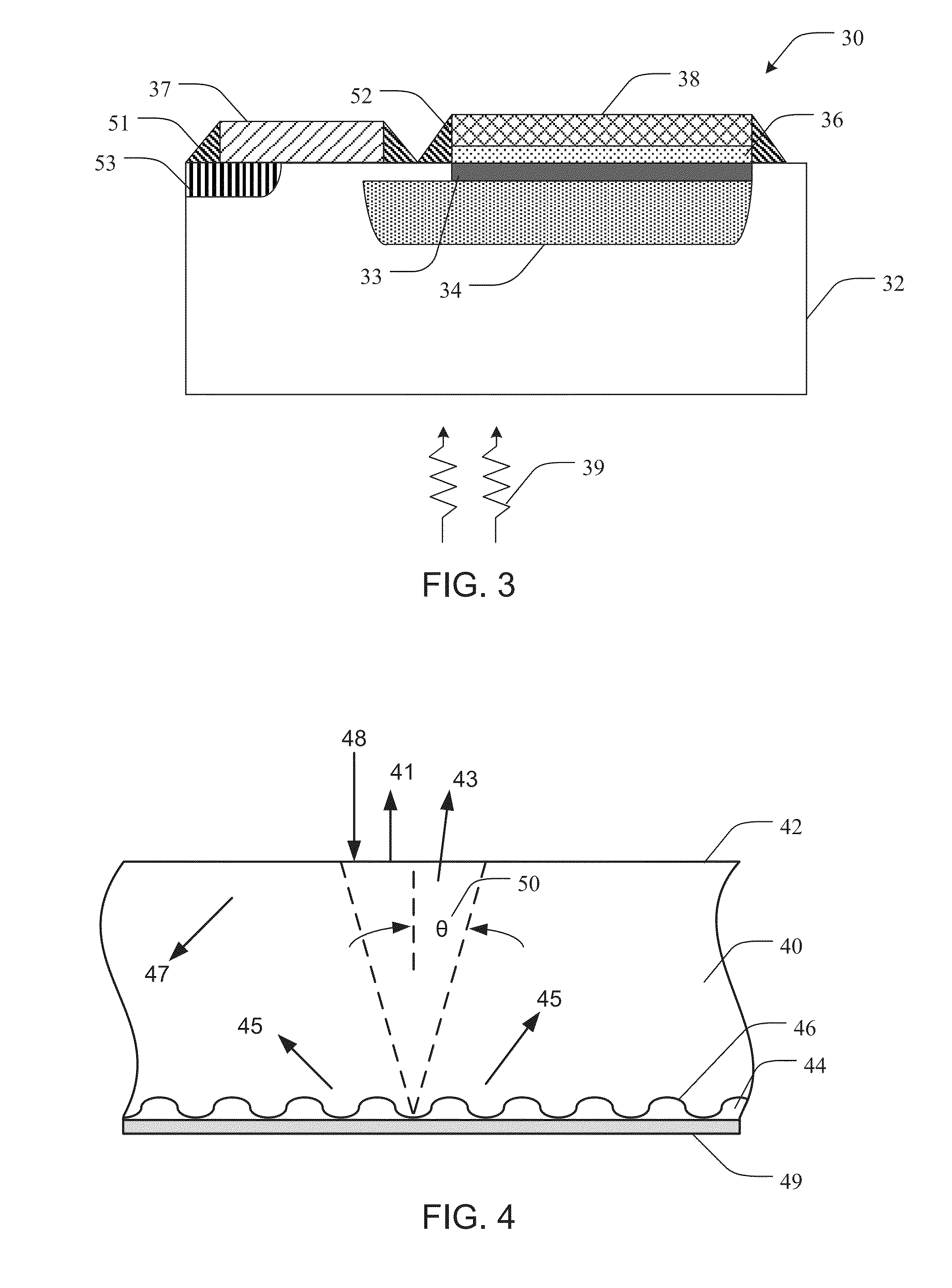
The present patent provides a backside-illuminated photosensitive imager device and methods of making it. The device includes a semiconductor substrate with multiple doped regions forming a junction, a textured region positioned to interact with electromagnetic radiation, and a passivation region positioned between the textured region and the junction. The passivation region isolates the junction from the textured region. The device also includes an electrical transfer element and a reflecting region positioned to reflect electromagnetic radiation. The textured region can have a surface morphology that directs electromagnetic radiation into the semiconductor substrate. The device can be used in various applications such as image sensors and optical devices.

Problems solved by technology

Silicon-based technologies for detecting infrared incident electromagnetic radiation have been problematic, however, because silicon is an indirect bandgap semiconductor having a bandgap of about 1.1 eV.

Method used


Image

  • Photosensitive imaging devices and associated methods
  • Photosensitive imaging devices and associated methods
  • Photosensitive imaging devices and associated methods

Examples


Embodiment Construction

[0023]Before the present disclosure is described herein, it is to be understood that this disclosure is not limited to the particular structures, process steps, or materials disclosed herein, but is extended to equivalents thereof as would be recognized by those ordinarily skilled in the relevant arts. It should also be understood that terminology employed herein is used for the purpose of describing particular embodiments only and is not intended to be limiting.

DEFINITIONS

[0024]The following terminology will be used in accordance with the definitions set forth below.

[0025]It should be noted that, as used in this specification and the appended claims, the singular forms “a,” and, “the” include plural referents unless the context clearly dictates otherwise. Thus, for example, reference to “a dopant” includes one or more of such dopants and reference to “the layer” includes reference to one or more of such layers.

[0026]As used herein, the terms “disordered surface” and “textured surfa...


PUM


Abstract

Backside illuminated photosensitive devices and associated methods are provided. In one aspect, for example, a backside-illuminated photosensitive imager device can include a semiconductor substrate having multiple doped regions forming a least one junction, a textured region coupled to the semiconductor substrate and positioned to interact with electromagnetic radiation, and a passivation region positioned between the textured region and the at least one junction. The passivation region is positioned to isolate the at least one junction from the textured region, and the semiconductor substrate and the textured region are positioned such that incoming electromagnetic radiation passes through the semiconductor substrate before contacting the textured region. Additionally, the device includes an electrical transfer element coupled to the semiconductor substrate to transfer an electrical signal from the at least one junction.

Description

PRIORITY DATA[0001]This application is a continuation of U.S. patent application Ser. No. 13 / 050,557, filed on Mar. 17, 2011, which is a continuation-in-part of U.S. patent application Ser. No. 12 / 885,158, filed on Sep. 17, 2010, which claims the benefit of U.S. Provisional Patent Application Ser. No. 61 / 243,434, filed on Sep. 17, 2009, U.S. Provisional Patent Application Ser. No. 61 / 311,004 filed on Mar. 5, 2010, and U.S. Provisional Patent Application Ser. No. 61 / 311,107, filed on Mar. 5, 2010, each of which is incorporated herein by reference. U.S. patent application Ser. No. 13 / 050,557 also claims the benefit of U.S. Provisional Application Ser. No. 61 / 443,988, filed on Feb. 17, 2011, which is incorporated herein by reference.BACKGROUND[0002]The interaction of light with semiconductor materials has been a significant innovation. Silicon imaging devices are used in various technologies, such as digital cameras, optical mice, video cameras, cell phones, and the like. Charge-couple...

Claims


Application Information

Patent Timeline
IPC IPC(8): H01L27/146H01L31/0232H01L31/0236H01L31/0352
CPCH01L27/14629H01L31/0236H01L31/0232H01L31/0352H01L27/14623H01L27/14625H01L27/1464H01L27/14645H01L27/14685H01L27/1461H01L27/1462H01L27/14689
Inventor HADDAD, HOMAYOONMCKEE, JEFFREYJIANG, JUTAOMILLER, DRAKEPALSULE, CHINTAMANIFORBES, LEONARD
Owner SIONYX
Learn More