Antenna device and electronic device

Active Publication Date: 2014-09-25
CASIO COMPUTER CO LTD
View PDF34 Cites 31 Cited by
  • Summary
  • Abstract
  • Description
  • Claims
  • Application Information

AI Technical Summary

Benefits of technology

[0014]The present invention is capable of narrowing the mounting space of an antenna device that is applied in various wireless communication, GPS, etc., and is capable of providing an a

Problems solved by technology

This decrease in size invites degradation in the performance of the wireless communication, such as degradation in electromagnetic-wave transmission and reception characteristics, and narrowing of the band of the elec

Method used


Image

  • Antenna device and electronic device
  • Antenna device and electronic device
  • Antenna device and electronic device

Examples


first embodiment

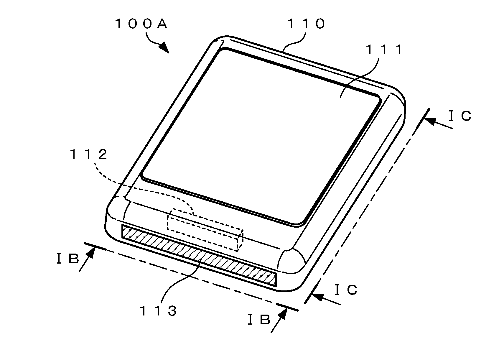
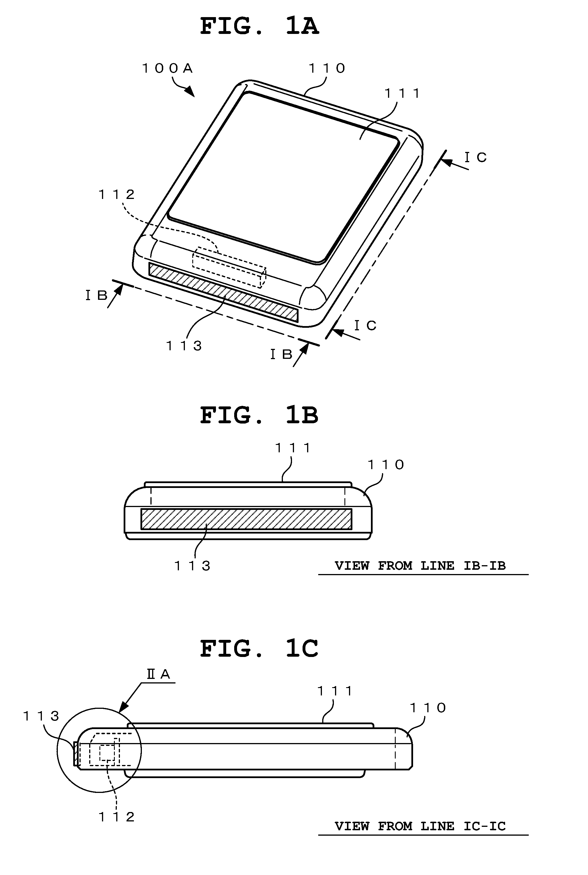
[0041]FIGS. 1A, 1B and 1C are schematic structural diagrams depicting a first embodiment in which an antenna device according to the present invention has been applied in an electronic device.

[0042]Here. FIG. 1A is a perspective view of the outer appearance structure of the electronic device according to the present embodiment. FIG. 1B is a diagram depicting a side surface of the electronic device when viewed from line IB-IB (for convenience of description, “I” is used herein as a sign corresponding to a Roman numeral of “1” depicted in FIGS. 1A, 1B, and 1C, and the same will apply hereinafter) in FIG. 1A.

[0043]FIG. 1C is a diagram depicting a side surface of the electronic device when viewed from line IC-IC in FIG. 1A.

[0044]Note that a conductive element in FIGS. 1A, 1B and 1C has been hatched so as to clarify the graphical representation for convenience of reference.

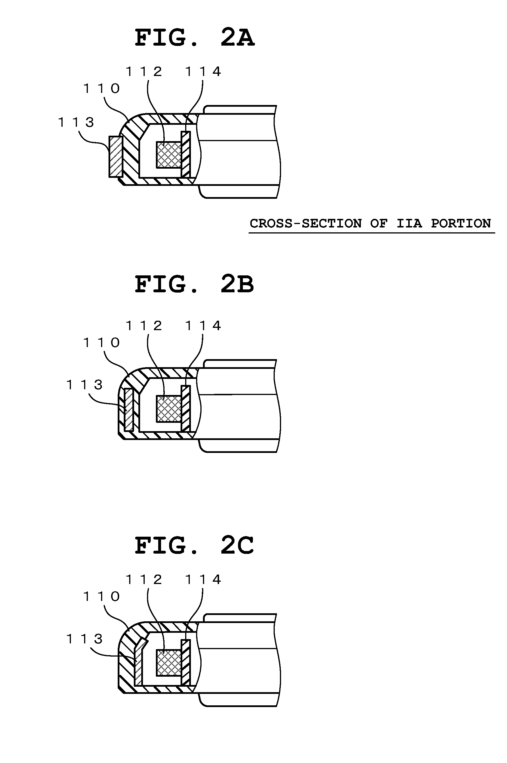
[0045]FIGS. 2A, 2B and 2C are enlarged sectional views of the main section of the electronic device according to the...

modification example of first embodiment

[0148]Next, a modification example of the first embodiment is described.

[0149]FIGS. 8A, 8B and 8C are schematic structure diagrams depicting a modification example of the electronic device in which the antenna device according to the first embodiment has been applied.

[0150]Here, FIG. 8A is a perspective view depicting the outer appearance structure of the electronic device according to the present embodiment.

[0151]FIG. 8B is a diagram depicting a side surface of the electronic device when viewed from line VIIIB-VIIIB (for convenience of description, “VIII” is used herein as a sign corresponding to a Roman numeral of “8” depicted in FIGS. 8A, 8B, and 8C, and the same will apply hereinafter) in FIG. 8A.

[0152]FIG. 8C is a diagram depicting a side surface of the electronic device when viewed from line IIIC-VIIIC in FIG. 8A.

[0153]FIGS. 9A, 9B and 9C are schematic structure diagrams depicting another modification example of the electronic device in which the antenna device according to th...

second embodiment

[0165]Next, a second embodiment of the electronic device in which the antenna device according to the present invention has been applied is described.

[0166]FIGS. 10A, 10B and 10C are schematic structure diagrams depicting the electronic device according to the second embodiment.

[0167]Here, FIG. 10A is a perspective view of the outer appearance structure of the electronic device according to the present embodiment.

[0168]FIG. 10B is a diagram depicting a side surface of the electronic device depicted in FIG. 10A when viewed from a belt section side.

[0169]FIG. 100 is a schematic view of a sectional structure of the electronic device taken along line XC-XC in FIG. 10B (for convenience of description, “X” is used herein as a sign corresponding to a Roman numeral of “10” depicted in FIGS. 10A to 10C).

[0170]Note that a conductive element in FIGS. 10A and 10B has been hatched so as to clarify the graphical representation for convenience of reference.

[0171]Also note that sections equivalent ...


PUM


Abstract

An antenna device of the present invention includes an antenna element which transmits or receives an electromagnetic wave having a specific frequency by being supplied with electric power, a conductive element which is formed of a conductive material, arranged so as to be spaced apart from and face the antenna element, and serves as a parasitic element, and a housing having a sealed space therein. The antenna element is provided inside the housing, and the conductive element is provided on outer surface of the housing, or in inner part of the housing, or in a mount member by which the housing is worn on a human body, or in a holding member for holding the housing; the conductive element is electromagnetically coupled to the antenna element, resonates with the specific frequency; and transmits or receives the electromagnetic wave.

Description

CROSS-REFERENCE TO RELATED APPLICATION[0001]This application is based upon and claims the benefit of priority from the prior Japanese Patent Application No. 2013-059429, filed Mar. 22, 2013, the entire contents of which are incorporated herein by reference.BACKGROUND OF THE INVENTION[0002]1. Field of the Invention[0003]The present invention relates to an antenna device and electronic device. Specifically, the present invention relates to an antenna device that is applied in a portable electronic device with a small-sized housing having a wireless communication function.[0004]2. Description of the Related Art[0005]In recent years, portable electronic devices including various wireless communication functions have been significantly widespread.[0006]Among various electronic devices such as smartphones (high-functionality portable telephones), tablet-type terminals, digital cameras, sports watches (running watches), and GPS devices for mountaineering, those having a function for connec...

Claims


Application Information

Patent Timeline
IPC IPC(8): H01Q1/24
CPCH01Q1/243H01Q1/273H01Q1/2283H01Q5/378H01Q5/385
Inventor AOKI, YUTAKAYAGI, SHIGERUYOSHIDA, KAORU
Owner CASIO COMPUTER CO LTD
Why Eureka
Try Eureka