Transistor using single crystal silicon nanowire and method for manufacturing same

Active Publication Date: 2014-12-04
KOREA UNIV RES & BUSINESS FOUND
View PDF3 Cites 28 Cited by
  • Summary
  • Abstract
  • Description
  • Claims
  • Application Information

AI Technical Summary

Benefits of technology

[0023]According to the present invention, by realizing the diameter of the single crystal silicon nanowire channel region used as the channel of the transistor to be smaller than the adjacent source region and the drain region, a transistor using a nanowire having a small source and drain parasitic resistance and excellent

Problems solved by technology

With respect to prior bottom-up methods for fabricating nanowires, there has been much progress in research in synthesizing nanowires, and its electrical, optical and physical characteristics, but there are still limitations in applying the methods for aligning this in desired locations in integrated systems.
On the contrary, overcoming problems with respect to alignments are possible when fabricating nanowires in a top-down method, but they are fabricated through SOI substrates and e-beam lithography and thus have problems in productivity of nanowire devices.
B

Method used


Image

  • Transistor using single crystal silicon nanowire and method for manufacturing same
  • Transistor using single crystal silicon nanowire and method for manufacturing same
  • Transistor using single crystal silicon nanowire and method for manufacturing same

Examples


Example

First Embodiment

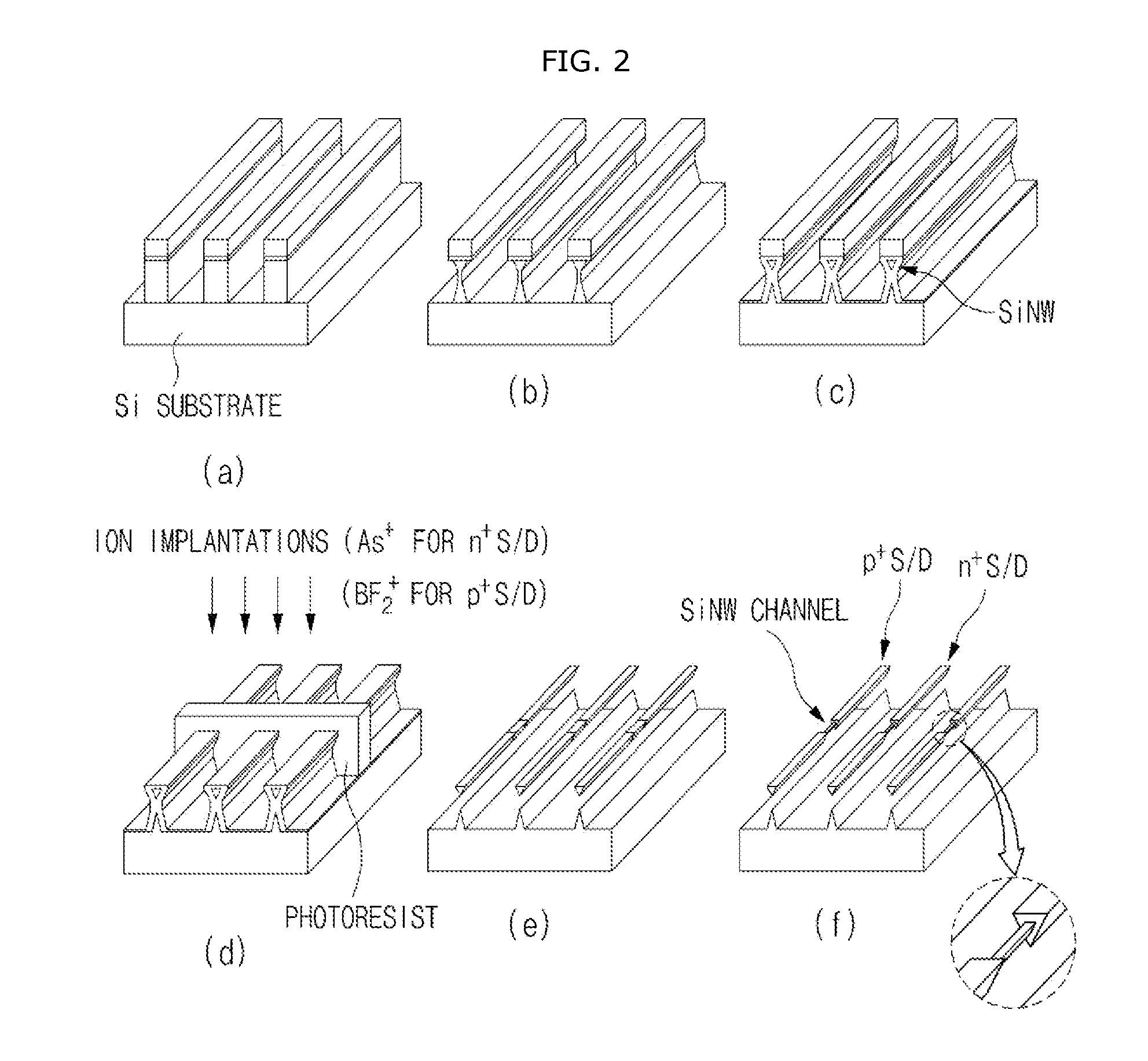
[0036]FIG. 2 is a process chart of fabricating a single crystal silicon nanowire in accordance with a first embodiment of the present invention.

[0037]In FIG. 2, a method for fabricating a single crystal silicon nanowire having a thin nanowire channel diameter by using an etch rate difference of an anisotropic we etching solution in accordance with an impurity concentration difference between a source / drain region in which high concentration impurities are implanted and a channel region in which low concentration impurities are implanted is illustrated.

[0038]First, after depositing a first thermal oxide film and a silicon nitride film on a single crystal silicon substrate having a crystal structure of (100), a silicon nanowire active pattern is formed through a photo process. And then, a silicon column structure is formed by an isotropic etching the silicon substrate through a silicon dry etching process by using the silicon nitride film as a mask (FIG. 2a).

[0039]And ...

Example

Second Embodiment

[0044]FIG. 3 is process chart of fabricating a single crystal silicon nanowire in accordance with a second embodiment of the present invention.

[0045]As illustrated in FIG. 3, in the method for fabricating the silicon nanowire having a thin channel diameter using the single crystal silicon substrate in accordance with a second embodiment of the present invention, by decreasing the diameter of the silicon nanowire channel region by growing the thermal oxide film after exposing the channel region of the nanowire, a single crystal silicon nanowire having a channel diameter in the level of several nm or several tens of nm is fabricated while maintaining the silicon nanowire diameter of the source / drain region, in which high concentration impurities are to be implanted, thick.

[0046]Here, since a portion of the process of the second embodiment is identical to FIG. 2a to FIG. 2b, hereinafter, the process for reducing the diameter of the silicon nanowire channel region is de...

Example

Third Embodiment

[0050]FIG. 4 is process chart of fabricating a single crystal silicon nanowire in accordance with a third embodiment of the present invention.

[0051]As illustrate in FIG. 4, in the method for fabricating the silicon nanowire having a thin channel diameter using the single crystal silicon substrate in accordance with a third embodiment of the present invention, by decreasing the diameter of the silicon nanowire channel region through a silicon dry etching by exposing only the channel region of the nanowire, a single crystal silicon nanowire having a channel diameter in the level of several nm or several tens of nm is fabricated while maintaining the silicon nanowire diameter of the source / drain region, in which high concentration impurities are to be implanted, thick.

[0052]Here, since a portion of the process of the third embodiment is identical to FIG. 2a to FIG. 2c, hereinafter, the process for reducing the diameter of the silicon nanowire channel region is described...


PUM


Abstract

A transistor using a single crystal silicon nanowire and a method for fabricating the transistor is disclosed. The transistor using a single crystal silicon nanowire comprises a substrate and a single crystal silicon nanowire formed on the substrate. Here, the single crystal silicon nanowire comprises a source region and a drain region formed longitudinally with the single crystal silicon nanowire and separate from each other, and a channel region located between the source region and the drain region, wherein the perpendicular thickness of the channel region to the longitudinal direction is thinner than the thickness of the source region and the drain region.

Description

TECHNICAL FIELD[0001]The present invention relates to a semiconductor device and a method for fabricating the same, and more particularly, a transistor using nanowire and a method for fabricating the transistor.BACKGROUND ART[0002]With respect to prior bottom-up methods for fabricating nanowires, there has been much progress in research in synthesizing nanowires, and its electrical, optical and physical characteristics, but there are still limitations in applying the methods for aligning this in desired locations in integrated systems.[0003]On the contrary, overcoming problems with respect to alignments are possible when fabricating nanowires in a top-down method, but they are fabricated through SOI substrates and e-beam lithography and thus have problems in productivity of nanowire devices.[0004]Recently, various methods regarding fabricating nanowires using single crystal silicon substrates, not SOI substrates, are being introduced, but devices using these are realized on rigid su...

Claims


Application Information

Patent Timeline
IPC IPC(8): H01L29/06H01L29/16H01L21/306H01L29/51H01L21/02H01L29/66H01L29/10
CPCH01L29/0673H01L29/66568H01L29/16H01L29/1033H01L21/30608H01L21/02532H01L21/02598H01L21/02164H01L21/0217H01L29/517B82Y10/00B82Y40/00H01L29/42392H01L29/66439H01L29/775H01L29/78696
Inventor KIM, SANGSIGLEE, MYEONG-WONJEON, YOUNGIN
Owner KOREA UNIV RES & BUSINESS FOUND
Why Eureka
Try Eureka