Field effect transistor

a field effect transistor and transistor technology, applied in the field of field effect transistors, can solve problems such as parasitic resistance, and achieve the effects of suppressing stress working between the second semiconductor layer and the first semiconductor layer, small parasitic resistance, and effective reduction of stress applied by the second semiconductor layer to the first semiconductor layer

Inactive Publication Date: 2007-08-02
PANASONIC CORP
View PDF12 Cites 16 Cited by
  • Summary
  • Abstract
  • Description
  • Claims
  • Application Information

AI Technical Summary

Benefits of technology

[0019]The third field effect transistor of this invention includes a first semiconductor layer made of a first group III-V nitride; a second semiconductor layer formed above the first semiconductor layer, made of a second group III-V nitride and having a gate recess portion; a third semiconductor layer that is formed between the second semiconductor layer and the first semiconductor layer, is made of a third group III-V nitride and absorbs stress caused between the second semiconductor layer and the first semiconductor layer; a gate electrode formed on the first semiconductor layer in the gate recess portion; and ohmic electrodes formed on the second semiconductor layer on both sides of the gate electrode.
[0020]In the third field effect transistor, stress applied by the second semiconductor layer to the first semiconductor layer can be effectively reduced. Therefore, an electron concentration in a channel region is minimally lowered beneath the gate recess side end of the second semiconductor layer, and hence, the field effect transistor attains small parasitic resistance.
[0021]In the third field effect transistor, the third semiconductor layer is preferably made of an amorphous film or a polycrystalline film. Thus, interstitial strain can be definitely absorbed by the third semiconductor layer, so that the stress working between the second semiconductor layer and the first semiconductor layer can be suppressed.
[0022]In the third field effect transistor, the third semiconductor layer is preferably grown at a lower growth temperature than the first semiconductor layer. Thus, the third semiconductor layer can be deposited without being influenced by crystal lattice so as to form a low-temperature-grown layer for absorbing the interstitial strain, and hence, the stress can be suppressed.
[0023]The fourth field effect transistor of this invention includes a first semiconductor layer made of a first group III-V nitride; a second semiconductor layer formed on the first semiconductor layer, made of a second group III-V nitride and having a gate recess portion; a gate electrode formed on the first semiconductor layer in the gate recess portion; ohmic electrodes formed on the second semiconductor layer on both sides of the gate electrode; and a stress reducing film for covering a bottom and a sidewall of the gate recess portion and causing stress in a direction for cancelling stress applied by the second semiconductor layer to the first semiconductor layer.
[0024]In the fourth field effect transistor, stress applied by the second semiconductor layer to the first semiconductor layer can be effectively reduced. Therefore, an electron concentration in a channel region is minimally lowered beneath the gate recess side end of the second semiconductor layer, and hence, the field effect transistor attains small parasitic resistance.

Problems solved by technology

Such a conventional semiconductor device in which an ohmic electrode is formed on a capping layer made of an n-type GaN layer, a superlattice layer including an AlGaN layer and a GaN layer or the like has, however, the following problem: It is necessary to form a gate electrode in a gate recess portion formed by removing the capping layer in the conventional semiconductor device.
Accordingly, the resistance of the channel region is increased, so as to disadvantageously increase the parasitic resistance.

Method used


Image

  • Field effect transistor
  • Field effect transistor
  • Field effect transistor

Examples


embodiment 1

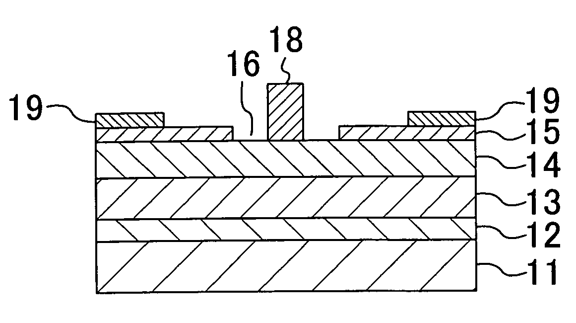
[0042]Embodiment 1 of the invention will now be described with reference to the accompanying drawings. FIG. 1 shows the cross-sectional structure of a field effect transistor (FET) according to Embodiment 1. As shown in FIG. 1, a buffer layer 12 made of aluminum nitride (AlN) or gallium nitride (GaN) grown at a low temperature is formed on a substrate 11 of sapphire. An active layer 13 of GaN, a barrier layer 14 of Al0.26Ga0.74N and a capping layer 15 made of a GaN layer doped with an n-type impurity and having lowered resistance are successively formed in this order in the upward direction on the buffer layer 12.

[0043]A gate recess portion 16 for exposing the barrier layer 14 therein is formed in the capping layer 15, and a gate electrode 18 is formed on the exposed portion of the barrier layer 14 in the gate recess portion 16. Two ohmic electrodes 19 respectively working as a source electrode and a drain electrode are formed on the capping layer 15 on both sides of the gate electr...

embodiment 2

[0058]Embodiment 2 of the invention will now be described with reference to the accompanying drawing. FIG. 7 shows the cross-sectional structure of an FET according to Embodiment 2 of the invention. In FIG. 7, like reference numerals are used to refer to like elements used in FIG. 1 so as to omit the description.

[0059]As shown in FIG. 7, in the FET of this embodiment, a capping layer 15 has a smaller thickness at a gate recess side end thereof than beneath an ohmic electrode 19. In other words, the thickness of the capping layer 15 is changed to be reduced in a stepwise manner toward the gate recess side end. The stress applied by the capping layer 15 to a barrier layer 14 is collected beneath a portion where the thickness of the capping layer 15 is changed, and the stress is larger as the change in the thickness of the capping layer 15 is larger. Accordingly, when the thickness of the capping layer 15 is changed in a stepwise manner, the stress applied by the capping layer 15 to th...

embodiment 3

[0068]Embodiment 3 of the invention will now be described with reference to the accompanying drawings. FIG. 9 shows the cross-sectional structure of an FET according to Embodiment 3 of the invention. In FIG. 9, like reference numerals are used to refer to like elements shown in FIG. 1 so as to omit the description.

[0069]As shown in FIG. 9, as a characteristic of the FET of this embodiment, a portion of a capping layer 15 corresponding to a sidewall of a gate recess portion 16 is nonlinearly reduced in the thickness in a downward convex curve so that the thickness change can be smaller toward a gate recess side end thereof. The FET of this embodiment may be regarded as one FET of Embodiment 2 where the thickness of the capping layer is changed in infinite stages.

[0070]The stress collection at the gate recess side end of the capping layer 15 is larger as an angle θ between the side face of the gate recess side end of the capping layer 15 and the top face of a barrier layer 14 is close...


PUM


Abstract

A field effect transistor includes a first semiconductor layer made of a first group III-V nitride; a second semiconductor layer formed on the first semiconductor layer, made of a second group III-V nitride and having a gate recess portion for exposing the first semiconductor layer therein; and a gate electrode formed on the first semiconductor layer in the gate recess portion. A product of stress applied by the second semiconductor layer to the first semiconductor layer and the thickness of the second semiconductor layer is 0.1 N/cm or less.

Description

CROSS-REFERENCE TO RELATED APPLICATIONS[0001]This application claims priority under 35 U.S.C. §119 on Patent Application No. 2006-020284 filed in Japan on Jan. 30, 2006 and Patent Application No. 2006-310131 filed in Japan on Nov. 16, 2006, the entire contents of which are hereby incorporated by reference.BACKGROUND OF THE INVENTION[0002]The present invention relates to a field effect transistor, and more particularly, it relates to a field effect transistor made of a group III-V nitride for use in a high-power and / or high-frequency device.[0003]A group III-V nitride semiconductor, such as gallium nitride (GaN), aluminum nitride (AlN), indium nitride (InN) or a mixed crystal represented by a general formula of (InxAl1-x)yGa1-yN (wherein 0≦x≦1 and 0≦y≦1), has physical characteristics of a wide band gap and a direct transition type band structure. Therefore, it is applied to an optical device by utilizing the physical characteristics. Furthermore, examination is being made on its appl...

Claims


Application Information

Patent Timeline
Patent Type & Authority Applications(United States)
IPC IPC(8): H01L29/15H01L31/00H01L29/739
CPCH01L29/2003H01L29/7843H01L29/7787
Inventor MURATA, TOMOHIROISHIDA, HIDETOSHI
Owner PANASONIC CORP
Why Eureka
Try Eureka