Imaging device and electronic apparatus

a technology of electronic equipment and electromagnetic field, which is applied in the direction of electrical equipment, semiconductor devices, photovoltaic energy generation, etc., can solve the problems of high and easy deformation of low-temperature sealing film. , to achieve the effect of reducing the thickness of light shielding film, reducing the stress of metal film, and high stress

Active Publication Date: 2020-09-24
SONY CORP
View PDF0 Cites 1 Cited by
  • Summary
  • Abstract
  • Description
  • Claims
  • Application Information

AI Technical Summary

Benefits of technology

[0085]In recent years, there has been developed an image sensor that is able to obtain photoelectric conversion signals of three colors with a single pixel. Such an image sensor is provided with, for example, two photodiodes (inorganic photoelectric conversion sections) stacked inside a silicon substrate, and an organic photoelectric conversion film above the silicon substrate. Moreover, in a general image sensor, an optical black region (OPB region) that detects black is formed around an effective pixel region. In the OPB region, a metal film such as W is formed as a light shielding film.
[0086]Now, as described above, an organic photoelectric conversion film varies greatly in characteristics under influences of stress of a film to be formed above. The light shielding film is formed in an upper layer than the organic photoelectric conversion film. The metal film that constitutes the light shielding film generally has high stress. Accordingly, there is possibility that the organic photoelectric conversion film generates an OPB level difference under influences of the stress of the light shielding film. A possible method to reduce the stress of the light shielding film is to reduce a thickness of the light shielding film. However, because the light shielding film is expected to have light shielding properties, it is difficult to reduce the stress by thinning.
[0087]Moreover, generally, the organic photoelectric conversion film is not resistant to heat. A sealing film provided between the light shielding film and the organic photoelectric conversion film is, therefore, formed by a low-temperature process. The sealing film is provided for prevention of intrusion of, for example, moisture into the organic photoelectric conversion film. The sealing film formed by the low-temperature process, having low film quality, is formed with a large thickness, in order to ensure the sealing properties. However, a distance from the organic photoelectric conversion film and the inorganic photoelectric conversion sections to the on-chip lens becomes larger by the thickness of the sealing film, causing a concern of a lowered oblique entrance characteristic.
[0088]Meanwhile, in this embodiment, the cavity structure 17A is formed in the sealing layer 17 at a position corresponding to the effective pixel region 100A. The sealing layer 17 is provided on the organic photoelectric conversion section 11G that includes the organic photoelectric conversion layer 15. Thus, stress applied to the organic photoelectric conversion layer 15 is reduced, while allowing for closer disposition of the exit surface of the on-chip lens 21 to the light receiving surface of each of the organic photoelectric conversion section 11G and the inorganic photoelectric conversion sections 11B and 11R. Hence, in the imaging device 1 of this embodiment, it is possible to enhance the photoelectric conversion characteristic, with the improvement in the oblique entrance characteristic, while maintaining the sealing properties and the light shielding properties.
[0089]Described next are second and third embodiments and modification examples (modification examples 1 and 2) of the forgoing first embodiment. It is to be noted that constituent elements corresponding to those of the imaging device 1 of the first embodiment are denoted by the same reference characters, and description thereof is omitted.

Problems solved by technology

But the metal film has high stress.
Moreover, generally, organic photoelectric conversion films are not resistant to heat.
However, the sealing film formed by the low-temperature process is easily degraded in film quality.

Method used


Image

  • Imaging device and electronic apparatus
  • Imaging device and electronic apparatus
  • Imaging device and electronic apparatus

Examples


modification example 1

2. Modification Example 1

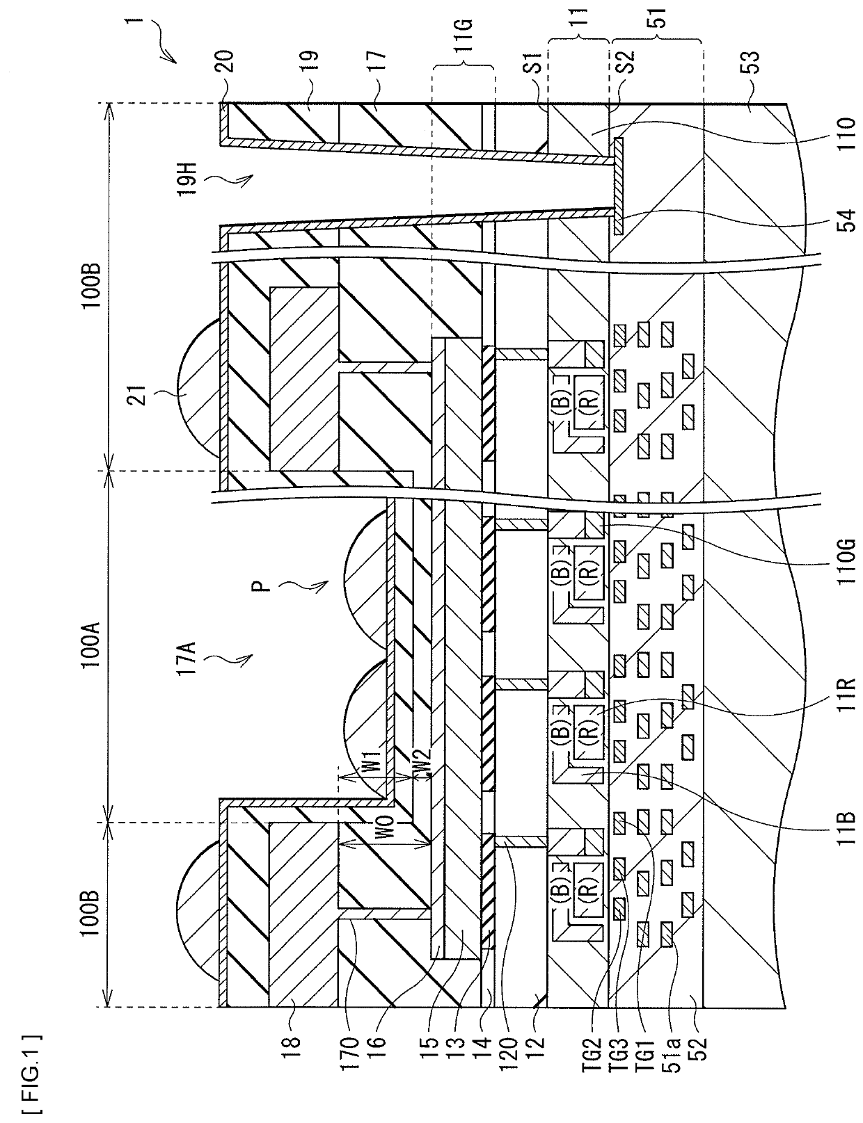
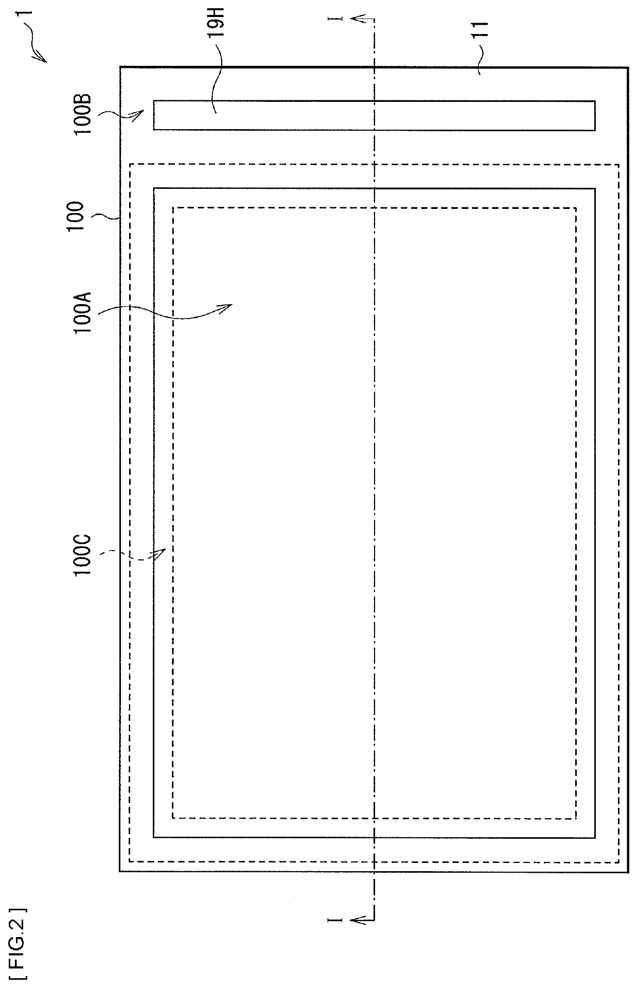
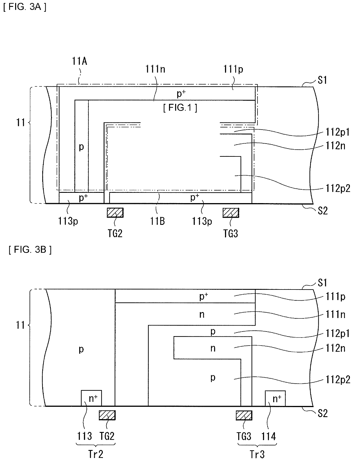
[0090]FIG. 7 illustrates a cross-sectional configuration of an imaging device (imaging device 2) according to a modification example (modification example 1) of the forgoing first embodiment. FIG. 8 illustrates a cross-sectional configuration of an imaging device (imaging device 3) according to the modification example of the forgoing first embodiment. As with the forgoing first embodiment, the imaging devices 2 and 3 are each, for example, a CCD image sensor or a CMOS image sensor of the backside illumination type (backside light receiving type), and each has the configuration in which the cavity structure 17A is provided at the position corresponding to the effective pixel region 100A. The imaging device 2 is different from the forgoing first embodiment in that the high sealing layer 20 is provided on the sealing layer 17. The imaging device 3 is different from the forgoing first embodiment in that the high sealing layer 20 is provided on the top electrode...

second embodiment

3. Second Embodiment

[0095]FIG. 9 illustrates a cross-sectional configuration of an imaging device (imaging device 4) according to a second embodiment of the disclosure. As with the forgoing first embodiment, the imaging device 4 is, for example, a CCD sensor or a CMOS sensor of the backside illumination type (backside light receiving type), and has a configuration in which the cavity structure 17A is provided at the position corresponding to the effective pixel region 100A, within the sealing layer 17 provided on the organic photoelectric conversion section 11G. In the imaging device 4 of this embodiment, a sealing layer 30 that differs in etching rate from the sealing layer 17 is provided at any position in a thickness direction inside the sealing layer 17.

[0096]As mentioned above, the sealing layer 30 is provided at any position in the thickness direction inside the sealing layer 17. The sealing layer 30 is a film having a different etching rate from that of the sealing layer 17, ...

modification example 2

4. Modification Example 2

[0099]FIG. 10 illustrates a cross-sectional configuration of an imaging device (imaging device 5) according to a modification example (modification example 2) of the forgoing second embodiment. As with the forgoing first embodiment and other example embodiments, the imaging device 5 is, for example, a CCD image sensor or a CMOS image sensor of the backside illumination type (backside light receiving type), and has a configuration in which the cavity structure 17A is provided at the position corresponding to the effective pixel region 100A. The imaging device of this modification example is a combination of the forgoing second embodiment with the imaging device 3 of the modification example 1, in which the sealing layer 30 having the different etching rate from that of the sealing layer 17 is provided on the top electrode 16 of the organic photoelectric conversion section 11G.

[0100]In this modification example, the sealing layer 30 is provided on the top elec...


PUM

PropertyMeasurementUnit
wavelength regionaaaaaaaaaa
thicknessaaaaaaaaaa

Abstract

An imaging device according to the disclosure includes: a semiconductor substrate including an effective pixel region in which a plurality of pixels are disposed, and a peripheral region provided around the effective pixel region; an organic photoelectric conversion layer provided on side of the semiconductor substrate on which a light receiving surface is disposed; a first sealing layer provided on the semiconductor substrate; a recess provided in the first sealing layer on the effective pixel region; and a light shielding film provided on the first sealing layer on the peripheral region.

Description

TECHNICAL FIELD[0001]The disclosure relates to an imaging device including an organic photoelectric conversion layer that uses an organic semiconductor material, and to an electronic apparatus.BACKGROUND ART[0002]In recent years, there has been progress in miniaturization of a pixel size in an imaging device such as a CCD (charge coupled device) image sensor or a CMOS (complementary metal oxide semiconductor) image sensor. The miniaturization of the pixel size causes reduction in the number of photons that enter a unit pixel, which contributes to lowered sensitivity as well as a lowered S / N ratio. Moreover, in a case where a color filter with a two-dimensional array of primary color filters of red, green and blue is used for colorization, light other than red light (color light of green and blue) is absorbed by the color filter, for example, in a red pixel, which brings about lowered sensitivity. Further, an interpolation process is performed between pixels upon generation of each c...

Claims


Application Information

Patent Timeline
Patent Type & Authority Applications(United States)
IPC IPC(8): H01L51/44H01L27/28H01L27/30
CPCH01L27/286H01L51/448H01L27/307H01L27/14623H01L27/14647H01L27/14667H01L27/14627H01L27/14605Y02E10/549H04N25/79H04N25/76H10K39/32H10K30/88H10K19/20
Inventor JOEI, MASAHIROIKEHARA, SHIGEHIROMANDA, SHUJI
Owner SONY CORP
Why Eureka
Try Eureka