
Radio frequency module
a frequency module and frequency technology, applied in the direction of printed circuits, non-printed electric components association, stress/warp reduction of printed circuits, etc., can solve the problems of increasing stress applied to electronic components, difficult for electronic components to be separated from mounting substrates, etc., to suppress the separation of electronic components and reduce the stress applied
- Summary
- Abstract
- Description
- Claims
- Application Information
AI Technical Summary
Benefits of technology
Problems solved by technology
Method used
Image

Examples
embodiment
[0016](1) Configuration of Radio Frequency Module
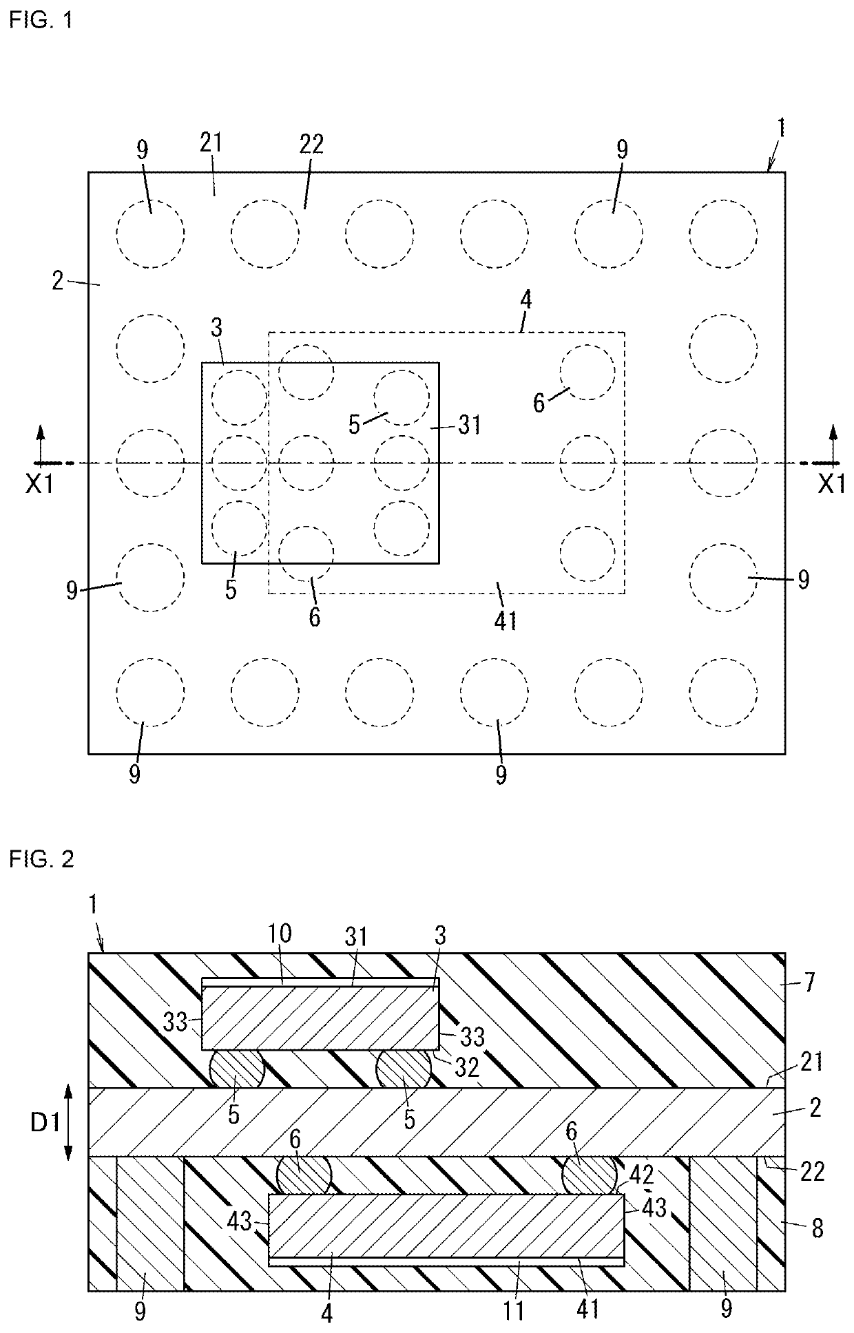
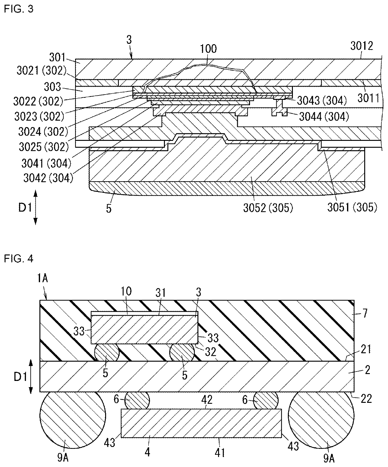
[0017]A configuration of a radio frequency module 1 according to the present embodiment will be described with reference to FIG. 1 to FIG. 3.
[0018]The radio frequency module 1 according to the present embodiment is used in, for example, a communication device. The communication device is, for example, a cellular phone such as a smartphone. Note that the communication device is not limited to a cellular phone, and may be, for example, a wearable terminal such as a smart watch.
[0019]The radio frequency module 1 can be electrically connected to an external substrate (not illustrated). The external substrate corresponds to, for example, a mother substrate of a cellular phone or a communication device. Here, a case where the radio frequency module 1 can be electrically connected to the external substrate includes not only a case where the radio frequency module 1 is directly mounted on the external substrate but also a case where the radio...
PUM
| Property | Measurement | Unit |
|---|---|---|
| thickness | aaaaa | aaaaa |
| stress | aaaaa | aaaaa |
| electrically | aaaaa | aaaaa |
Abstract
Description
Claims
Application Information