Dual emission type display panel
a display panel and dual emission technology, applied in the field of display panels, can solve the problems of high manufacturing cost of the resultant dual emission type organic light emitting display and the significant thickness of the display panel, and achieve the effect of improving resolution
- Summary
- Abstract
- Description
- Claims
- Application Information
AI Technical Summary
Benefits of technology
Problems solved by technology
Method used
Image
Examples
first embodiment
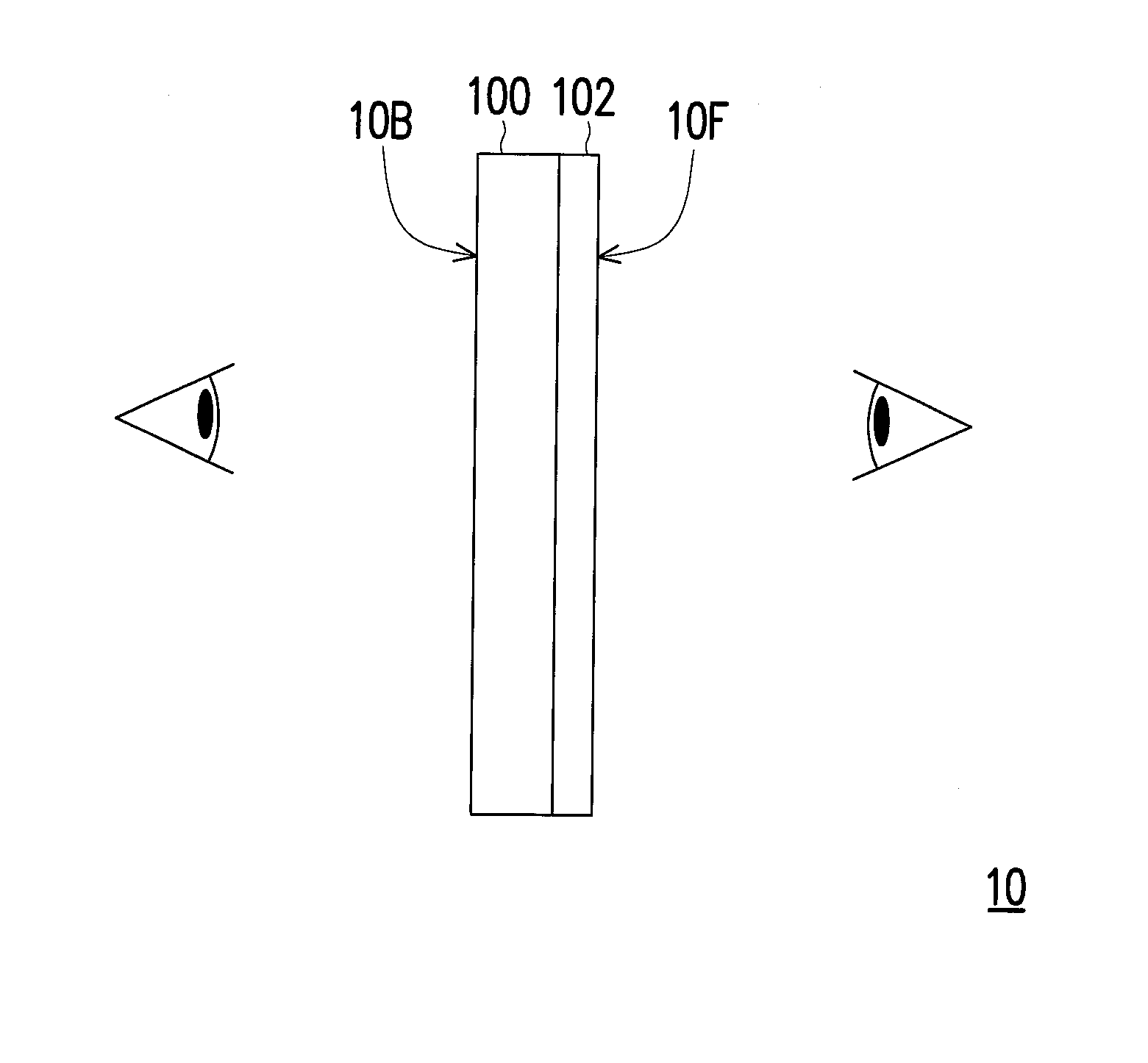
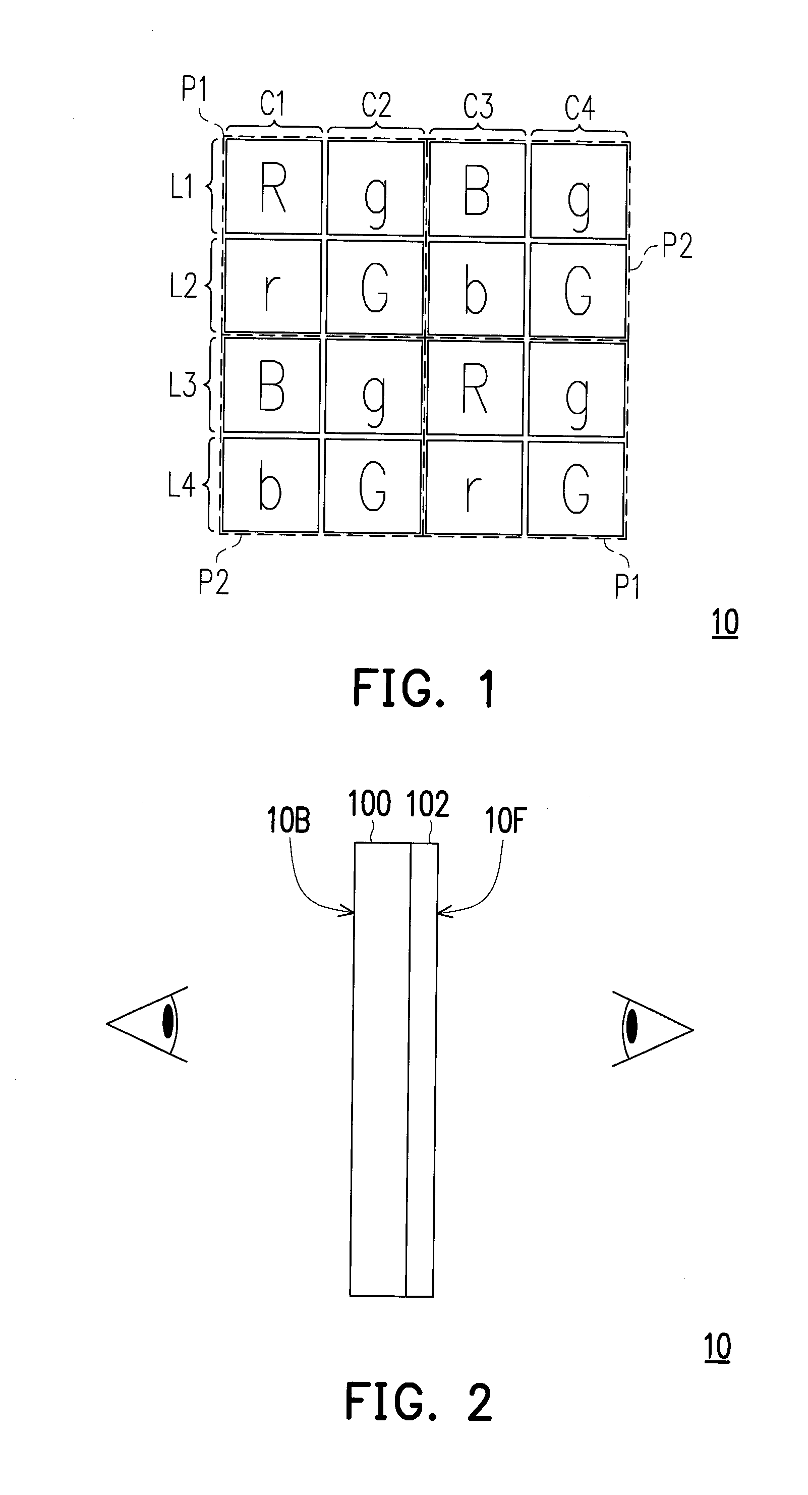
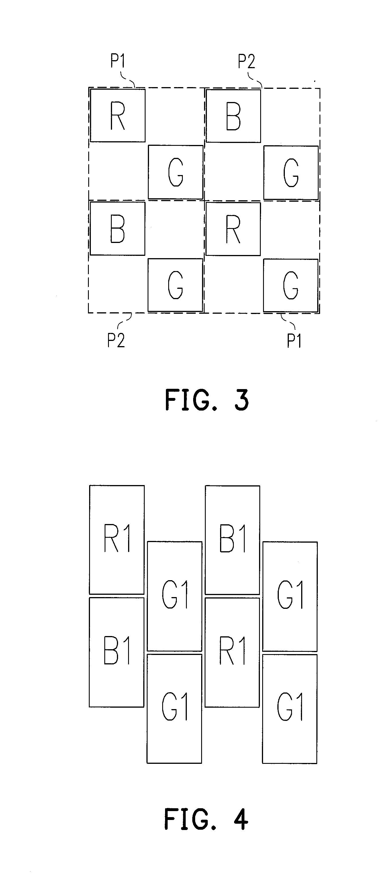
[0029]FIG. 1 is a schematic view illustrating a dual emission type display panel according to the invention. FIG. 2 is a schematic side view illustrating the dual emission type display panel depicted in FIG. 1. FIG. 3 is a schematic view illustrating a front viewing surface of the dual emission type display panel in FIG. 1. FIG. 4 is a schematic equivalent view illustrating the front viewing surface of the dual emission type display panel in FIG. 3. FIG. 5 is a schematic view illustrating a rear viewing surface of the dual emission type display panel in FIG. 1. FIG. 6 is a schematic equivalent view illustrating the rear viewing surface of the dual emission type display panel in FIG. 5.
[0030]With reference to FIG. 1 and FIG. 2, the dual emission type display panel 10 described in the present embodiment has a front viewing surface 10F and a rear viewing surface 10B. That is, a user is able to observe images displayed by the dual emission type display panel 10 through the front viewing...
second embodiment
[0039]FIG. 7 is a schematic view illustrating a dual emission type display panel according to the invention. FIG. 8 is a schematic side view illustrating the dual emission type display panel depicted in FIG. 7. FIG. 9 is a schematic view illustrating a front viewing surface of the dual emission type display panel in FIG. 7. FIG. 10 is a schematic equivalent view illustrating the front viewing surface of the dual emission type display panel in FIG. 9. FIG. 11 is a schematic view illustrating a rear viewing surface of the dual emission type display panel in FIG. 7. FIG. 12 is a schematic equivalent view illustrating the rear viewing surface of the dual emission type display panel in FIG. 11.
[0040]With reference to FIG. 7 and FIG. 8, the dual emission type display panel 20 described in the present embodiment has a front viewing surface 20F and a rear viewing surface 20B. That is, a user is able to observe images displayed by the dual emission type display panel 20 through the front vie...
fourth embodiment
[0068]FIG. 15 is a schematic cross-sectional view illustrating one top emission pixel unit and one bottom emission pixel unit in a dual emission type display panel according to the invention.
[0069]With reference to FIGS. 15 and 14, the dual emission type display panel 40 shown in FIG. 15 is similar to the dual emission type display panel 30 shown in FIG. 14, and therefore identical devices are marked by the same reference numbers and will not be repeated. The difference between the dual emission type display panels 40 and 30 lies in that the thin metal material 407 constituting the reflective cathode 506′ in the bottom emission pixel unit 500 of the dual emission type display panels 40 is stacked onto the thick metal material 507, while the thick metal material 507 in the bottom emission pixel unit 500 of the dual emission type display panels 30 is stacked onto the thin metal material 407 that constitutes the reflective cathode 506 in the bottom emission pixel unit 500 of the dual e...
PUM
 Abstract
Description
Claims
Application Information


