Base Substrate Which Prevents Burrs Generated During the Cutting Process and Method for Manufacturing the Same

a technology of cutting process and base substrate, which is applied in the direction of printed circuit aspects, printed circuit non-printed electrical components association, conductive pattern formation, etc., can solve problems such as electrical short generation, and achieve the effect of minimizing or eliminating the generation of burrs

Active Publication Date: 2015-02-19
POINT ENG
View PDF3 Cites 6 Cited by
  • Summary
  • Abstract
  • Description
  • Claims
  • Application Information

AI Technical Summary

Benefits of technology

[0019]It is an advantage if no burrs are generated during the separation process of the optical device from the base substrate i.e. sawing or dicing process. By forming predetermined through-holes covering the insulation layer with respect to the cut surface of the optical device generation of burrs can be minimized or eliminated.

Problems solved by technology

However, according to the conventional methods, burrs are generated during the sawing process or the dicing process, and there has been a problem of generating an electrical short due to the situation wherein the burrs, which are generated due to the difference in the hardness between the material constituting the conductive layer and the material constituting the insulation layer, are crossing over the insulation layer and the like.

Method used


Image

  • Base Substrate Which Prevents Burrs Generated During the Cutting Process and Method for Manufacturing the Same
  • Base Substrate Which Prevents Burrs Generated During the Cutting Process and Method for Manufacturing the Same
  • Base Substrate Which Prevents Burrs Generated During the Cutting Process and Method for Manufacturing the Same

Examples


Embodiment Construction

Technical Problem

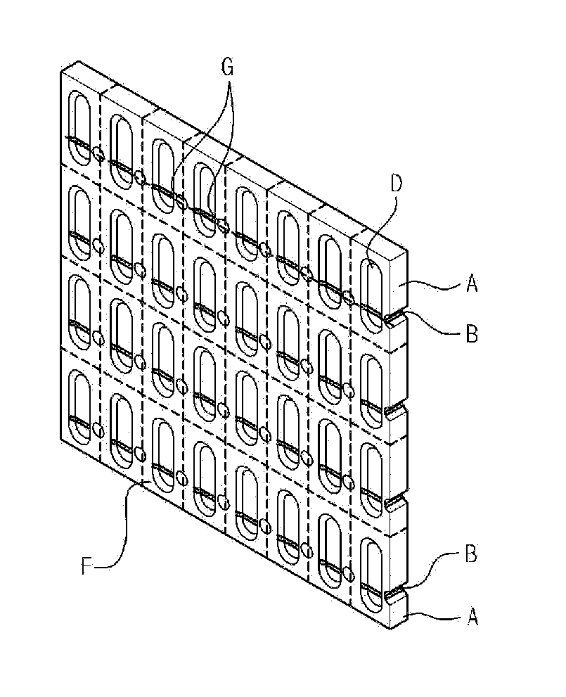
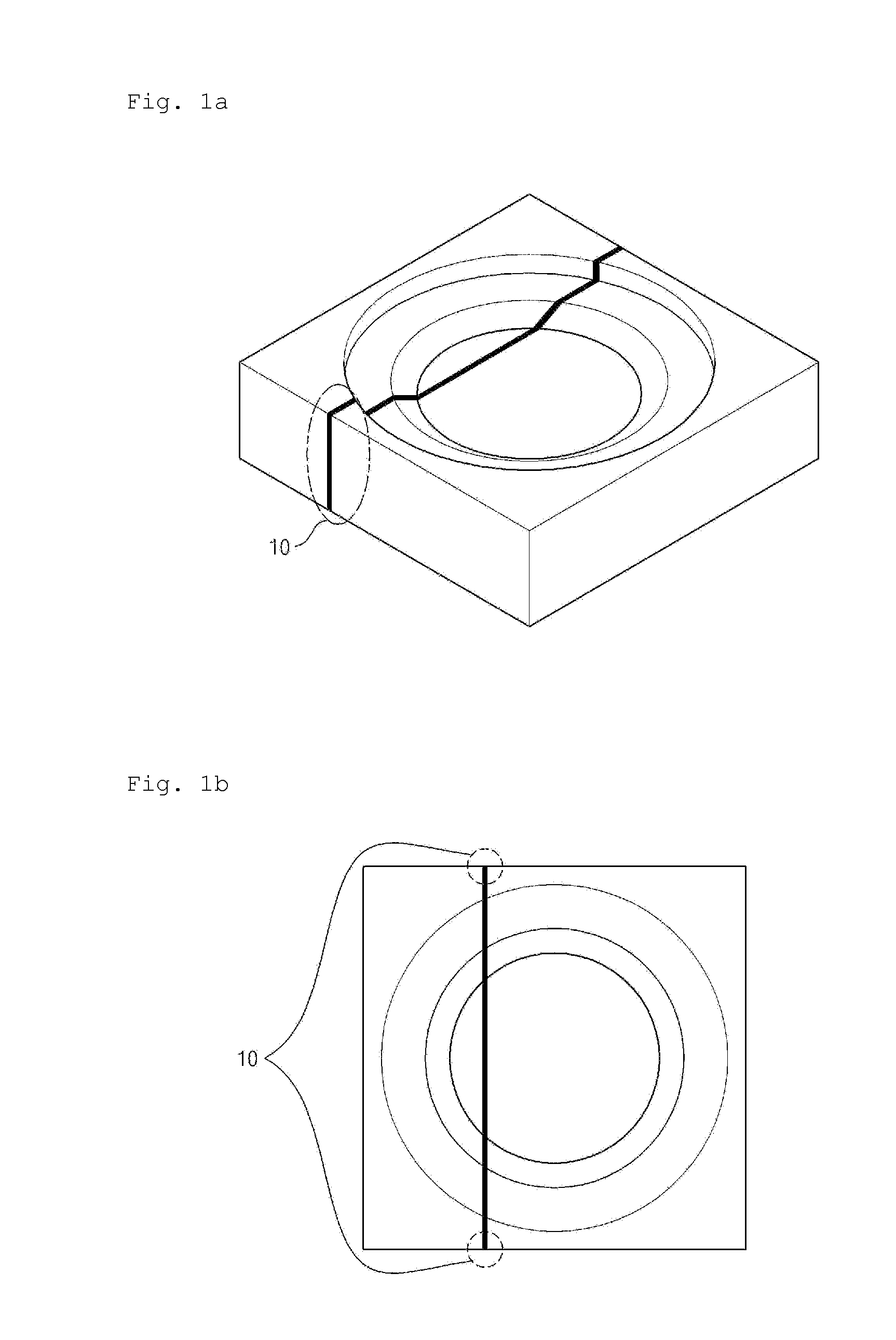
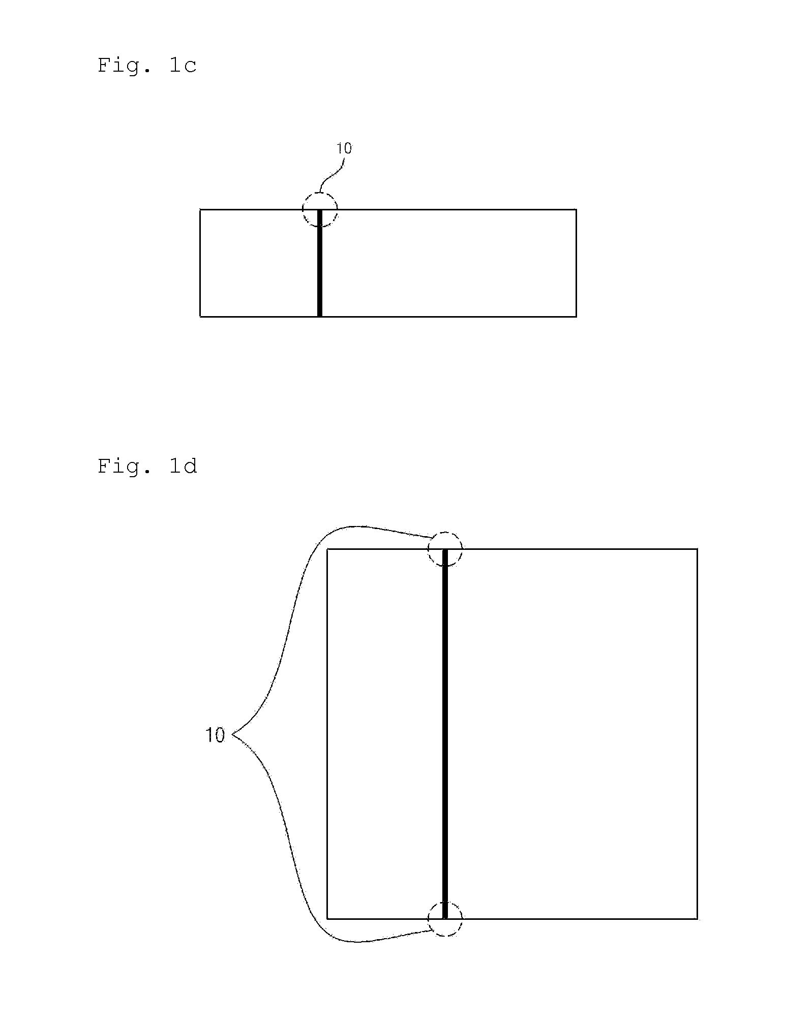
[0006]Embodiments of the present invention suggest solving the above described problems of the prior art by providing a configuration of a base substrate which may not generate burrs during the separation process of the optical devices from the base substrate, i.e. a sawing or a dicing process.

[0007]More particularly, the purpose is to provide a configuration which may not generate burrs during the separation process of the optical device by forming a predetermined through-hole with respect to the cross-section of the optical device.

Solution to Problem

[0008]To solve the above described problems, a base substrate which prevents burrs generated during the cutting process includes: multiple conductive layers stacked in one direction with respect to the base substrate; at least one insulation layer being alternately stacked with said conductive layers and electrically separating said conductive layers; and a through-hole penetrating said base substrate covering said ins...


PUM

PropertyMeasurementUnit
conductiveaaaaaaaaaa
depthaaaaaaaaaa
hardnessaaaaaaaaaa

Abstract

A base substrate which prevents burrs generated during the cutting process includes: multiple conductive layers stacked in one direction with respect to the base substrate; at least one insulation layer being alternately stacked with said conductive layers and electrically separating said conductive layers; and a through-hole penetrating said base substrate covering said insulation layer at the contact region where said cut surface and said insulation layer meet during the cutting of said base substrate in accordance with a predetermined region of the chip substrate. A method of manufacturing the base substrate includes alternately stacking conductive layers and insulation layers and forming a through-hole.

Description

[0001]The present application claims priority from Korean application no. 10-2013-0097185, filed Aug. 16, 2013, the full disclosure of which is hereby incorporated by reference herein.TECHNICAL FIELD[0002]The present invention relates to a base substrate and a method for manufacturing the same, more particularly to a base substrate where the optical device chips are mounted thereon.BACKGROUND ART[0003]LED is being used as the light source of a back light unit (BLU) for a liquid crystal display (LCD) which is used in the flat panel displays such as TVs, computer monitors, and the like.[0004]An optical device chip such as an LED is being mounted on the base substrate for an optical device, and the individual optical devices are manufactured through a separation process i.e. sawing or dicing of the base substrate for the optical devices.[0005]However, according to the conventional methods, burrs are generated during the sawing process or the dicing process, and there has been a problem...

Claims


Application Information

Patent Timeline
Patent Type & Authority Applications(United States)
IPC IPC(8): H05K3/00H05K3/46H05K1/18
CPCH05K3/0052H05K2201/10121H05K3/4697H05K1/183H01L33/48H01L33/62H01L2924/0002H05K2201/10106Y10T29/49155H01L2924/00H01L21/02H01L21/30H01L33/00H05K2201/09718H05K2201/09827H05K2201/09845H05K2201/09854H05K2201/09863H05K2201/10
Inventor AHN, BUM MOPARK, SEUNG HOYUN, KYOUNG JA
Owner POINT ENG
Why Eureka
Try Eureka