Sensor device

a sensor and device technology, applied in the field of sensor devices, can solve problems such as contamination during device singulation, and achieve the effect of easing the singulation of the sensor devi

Active Publication Date: 2015-05-28
SENSIRION AG
View PDF8 Cites 8 Cited by
  • Summary
  • Abstract
  • Description
  • Claims
  • Application Information

AI Technical Summary

Benefits of technology

[0024]In a preferred embodiment, prior to separating the sensor support assembly into sensor devices, top elements are deposited on parts of the venting medium. The top elements may contain alignment and / or separation marks which aid the separation also referred to as singulation. The top elements may also ease sensor device singulation and protect the venting medium during and after singulation. Additionally, the top elements may be processed with labels, e.g. detailing the device type or the individual device, either before or after the singulation process.

Problems solved by technology

When a sensor device is manufactured, especially in a batch process, there may be contaminations arising during device singulation, e.g. by sawing or laser cutting.

Method used


Image

  • Sensor device
  • Sensor device
  • Sensor device

Examples


Embodiment Construction

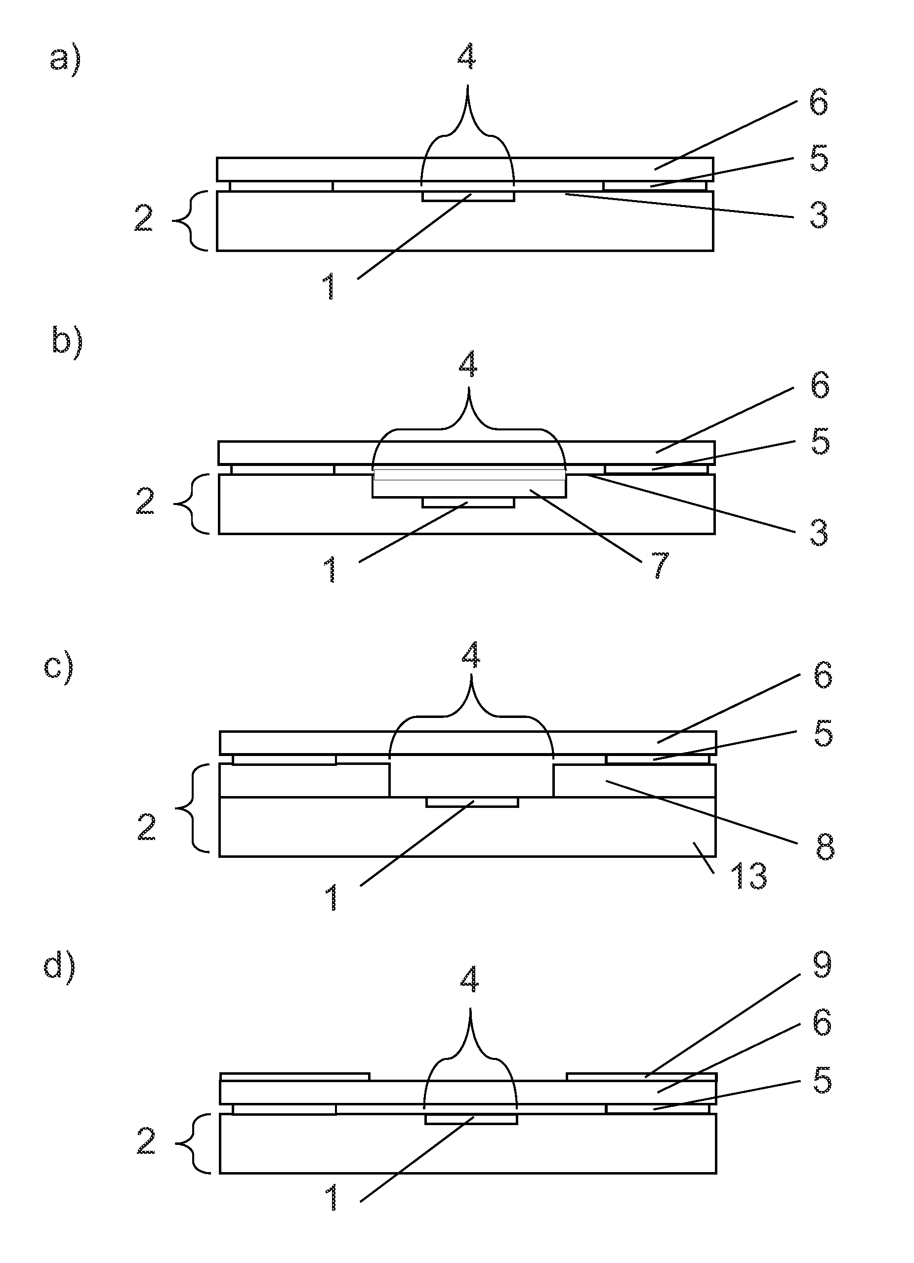
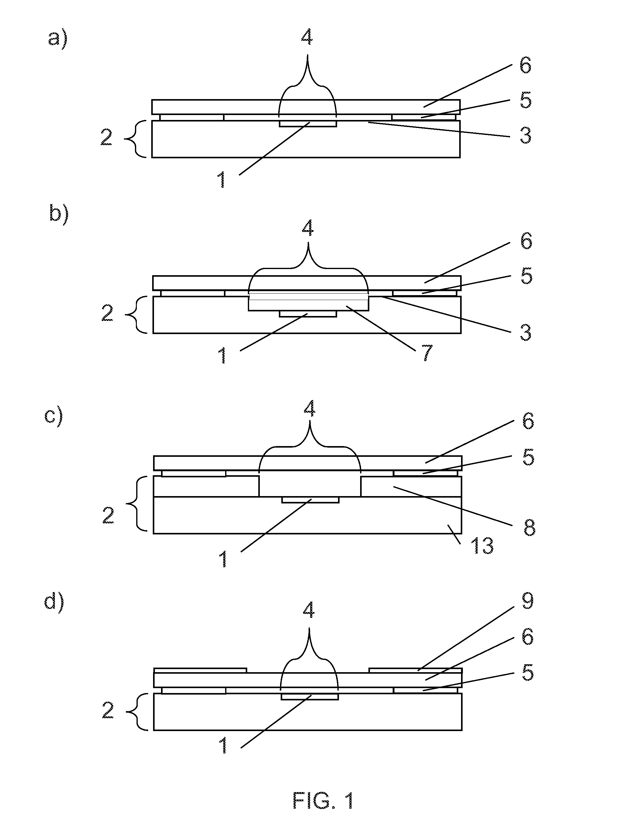
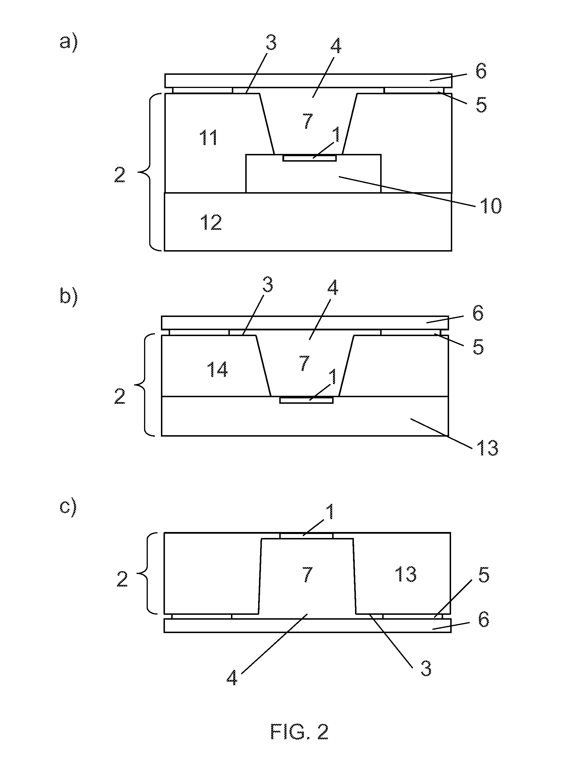
[0034]FIG. 1a) shows a schematic sectional view of a sensor device in accordance with an embodiment of the present invention. The sensor device includes a sensitive element 1, which is integrated in a support 2. In this embodiment, the support 2 is a semiconductor substrate, e.g. a silicon substrate, and it may include additional features, such as a heater structure, a suspended membrane, an integrated processing circuit, through silicon vias and solder balls. The gas to be sensed can enter the sensitive element 1 via the access opening 4 which is located in a surface 3 of the support 2. Parts of the surface 3 are covered by a layer of adhesive material 5. A venting medium 6 extends over the entire surface 3 of the support 2 and the access opening 4 and is attached to the support 2 by the layer of adhesive material 5.

[0035]FIG. 1b) shows another embodiment of a sensor device in accordance with the present invention. In this embodiment, the sensitive element 1 is located in a cavity ...


PUM

PropertyMeasurementUnit
thicknessaaaaaaaaaa
conductiveaaaaaaaaaa
thermal insulationaaaaaaaaaa

Abstract

A sensor device comprises a sensitive element (1) and a support (2) for the sensitive element, the support having a surface (3) with an access opening (4) to the sensitive element (1). A layer of adhesive material (5) covers at least parts of the surface (3). A venting medium (6) extends over the entire surface (3) of the support (2) and the access opening (4) and is attached to the support (2) by the layer of adhesive material (5).

Description

CROSS REFERENCE TO RELATED APPLICATIONS[0001]This application claims the priority of European patent application 13005237.6, filed on November 6, 2013, the disclosure of which is incorporated herein by reference in its entirety.FIELD OF THE INVENTION[0002]The present invention relates to a sensor device and a method for manufacturing a sensor device.BACKGROUND OF THE INVENTION[0003]Sensor devices and methods for manufacturing sensors devices are known. In the European patent application no. EP 2 481 703 A1 for example, there is described a method for manufacturing a sensor device, wherein a spacer is arranged at the front side of a substrate at which front side a sensitive element is arranged, too. Holes are etched for building vias extending through the substrate between the front side of the substrate and its back side. After etching, the holes are filled with conductive material to complete the vias. The spacer provides protection to the sensitive element and the sensor device th...

Claims


Application Information

Patent Timeline
Patent Type & Authority Applications(United States)
IPC IPC(8): G01N33/00
CPCG01N2033/0095G01N33/0009B81B7/0029B81C1/00896Y10T156/1052
Inventor HUNZIKER, WERNERBRAUN, STEPHAN
Owner SENSIRION AG
Why Eureka
Try Eureka