Manufacturing method of display device

Inactive Publication Date: 2015-05-28
JAPAN DISPLAY INC
View PDF3 Cites 5 Cited by
  • Summary
  • Abstract
  • Description
  • Claims
  • Application Information

AI Technical Summary

Benefits of technology

[0007]According to the manufacturing method of the display device described in JP 2005-148335 A, on the metal foil of the evaporation mask, the stronger tension from the frame acts in the part farther away from the corner of the frame. Accordingly,

Problems solved by technology

That may cause reduction in accuracy of the positions in

Method used


Image

  • Manufacturing method of display device
  • Manufacturing method of display device
  • Manufacturing method of display device

Examples


Example

[0025]As below, as an example of a manufacturing method of a display device according to one embodiment of the invention, a manufacturing method of an organic electro luminescent display device will be explained with reference to the drawings. Note that the drawings for reference in the following explanation may enlarge and show characteristic parts for convenience for making the characteristics understandable, and the dimension ratios etc. of the respective component elements are not necessarily the same as the actual dimension ratios. Further, the materials etc. exemplified in the following explanation are just examples, and the respective component elements may be different from those and may be changed and implemented in a range in which the scope of the invention is unchanged.

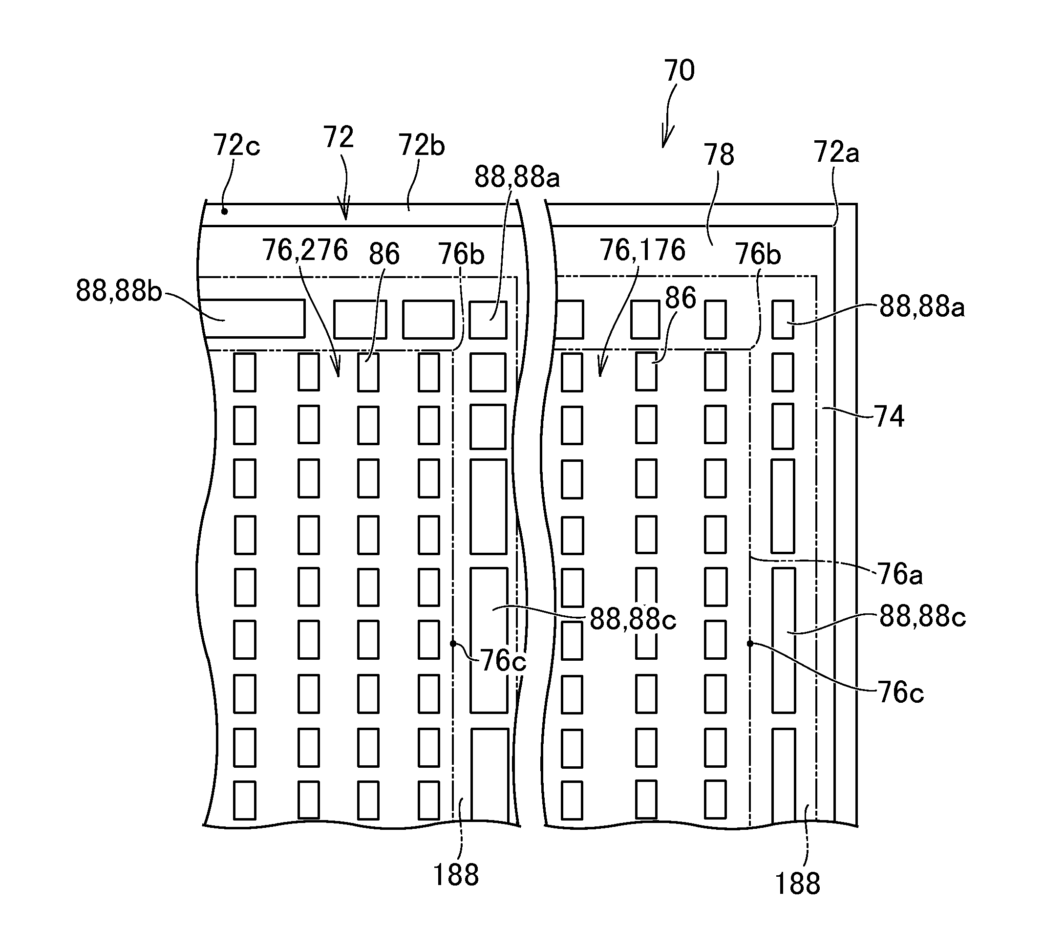
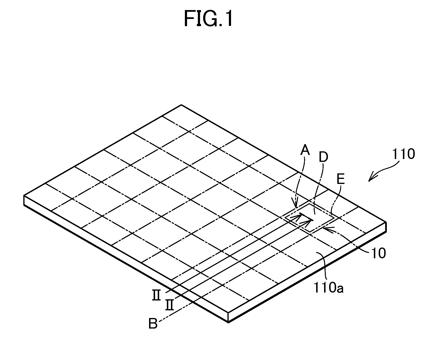
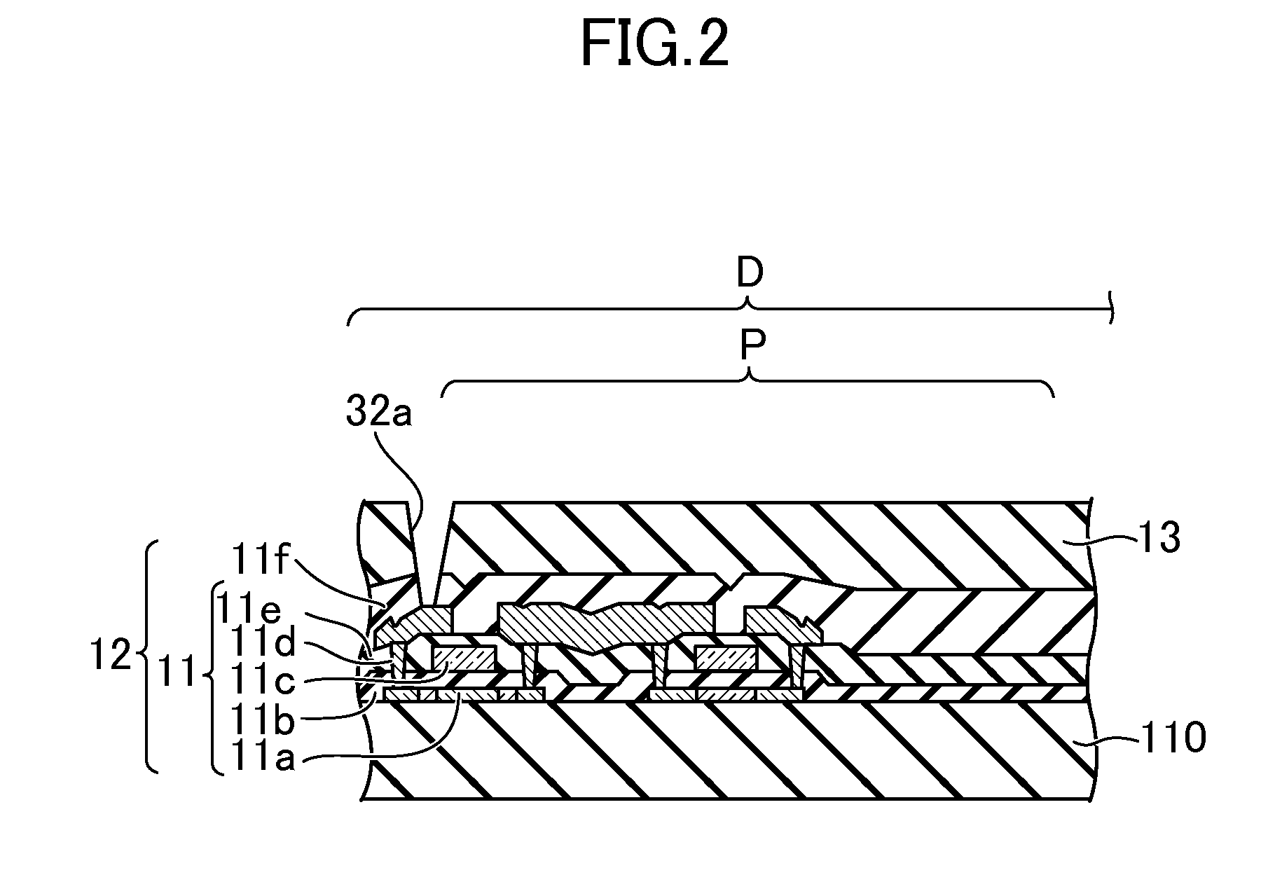
[0026]First, a mother substrate 110 is prepared. FIG. 1 is a schematic perspective view of the mother substrate 110 showing a manufacturing method of a display device (organic electro luminescent display d...


PUM

PropertyMeasurementUnit
Thicknessaaaaaaaaaa
Shapeaaaaaaaaaa
Areaaaaaaaaaaa

Abstract

A manufacturing method of a display device of the invention includes a step of forming an organic layer in correspondence with respective pixels on a substrate having a display area and a non-display area, the step of forming the organic layer includes a step of depositing a material of the organic layer using a mask having a frame-like frame and a mask foil fixed to the frame, the mask foil has openings provided in an area corresponding to the display area and dummy holes provided along an outer periphery of the area corresponding to the display area in an area corresponding to the non-display area, and an area of a plan view shape of the dummy hole adjacent to a midpoint of a side of the outer periphery is larger than an area of a plan view shape of the dummy hole adjacent to a corner of the outer periphery.

Description

CROSS-REFERENCE TO RELATED APPLICATION[0001]The present application claims priority from Japanese application JP 2013-243788 filed on Nov. 26, 2013, the content of which is hereby incorporated by reference into this application.BACKGROUND OF THE INVENTION[0002]1. Field of the Invention[0003]This invention relates to a manufacturing method of a display device.[0004]2. Description of the Prior Art[0005]As thinner and lighter light emitting sources, organic electro luminescent elements have received attention and display devices including many organic electro luminescent elements have been developed. The organic electro luminescent element has a structure in which an organic layer having a light emitting layer is sandwiched between a lower electrode and an upper electrode.[0006]As a manufacturing method of the display device, in JP 2005-148335 A, a method of evaporating an organic layer on a substrate having a display area and a non-display area using an evaporation mask of a metal foi...

Claims


Application Information

Patent Timeline
IPC IPC(8): H01L51/56
CPCH01L51/56C23C14/042H10K71/166H10K71/00
Inventor OOKAWARA, TAKESHI
Owner JAPAN DISPLAY INC
Why Eureka
Try Eureka