Cell Layout for SRAM FinFET Transistors

Active Publication Date: 2015-07-23
TAIWAN SEMICON MFG CO LTD
View PDF5 Cites 43 Cited by
  • Summary
  • Abstract
  • Description
  • Claims
  • Application Information

AI Technical Summary

Problems solved by technology

However, the smaller feature size may lead to more leakage current.
However, as semiconductor devices keep shrinking, due to the short channel leakage effect, the gate cannot fully control the channel region, especially a further portion of the channel region to cut off t

Method used


Image

  • Cell Layout for SRAM FinFET Transistors
  • Cell Layout for SRAM FinFET Transistors
  • Cell Layout for SRAM FinFET Transistors

Examples


Embodiment Construction

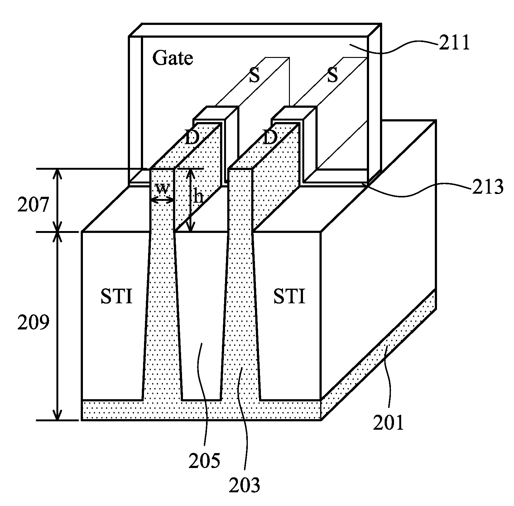
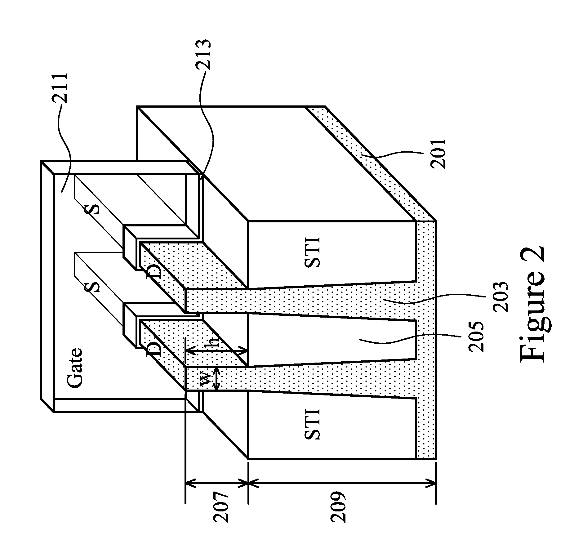
[0023]The making and using of the present embodiments are discussed in detail below. It should be appreciated, however, that the present disclosure provides many applicable inventive concepts that can be embodied in a wide variety of specific contexts. The specific embodiments discussed are merely illustrative of specific ways to make and use the embodiments of the disclosure, and do not limit the scope of the disclosure.

[0024]The present disclosure will be described with respect to embodiments in a specific context, a static random-access memory (SRAM) formed of fin field effect transistors (FinFETs). The embodiments of the disclosure may also be applied, however, to a variety of semiconductor devices. Various embodiments will be explained in detail with reference to the accompanying drawings.

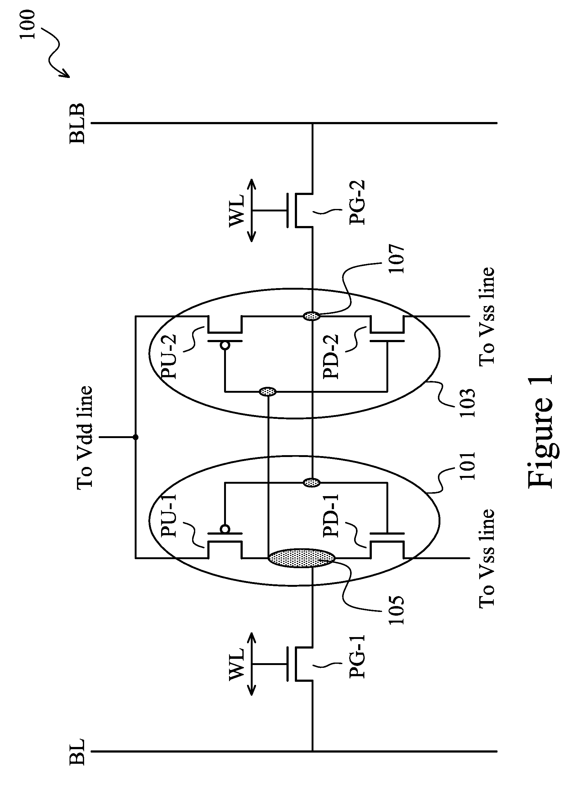
[0025]Static random-access memory (SRAM) is a type of volatile semiconductor memory that uses bistable latching circuitry to store each bit. Each bit in an SRAM is stored on four transistors (...


PUM


Abstract

An SRAM array and method of making is disclosed. Each SRAM cell comprises two pull-up (PU), two pass-gate (PG), and two pull-down (PD) FinFETs. The PU transistors are adjacent to each other and include one active fin having a first fin width. Each PG transistor shares at least one active fin with a PD transistor. The active fin shared by a PG and a PD transistor has a second fin width smaller than the first fin width. The method includes patterning a plurality of fins including active fins and dummy fins and patterning and removing at least a portion of the dummy fins. No dummy fin is disposed between PU FinFETs in a memory cell. One dummy fin is disposed between a PU FinFET and the at least one active fin shared by a PG and a PD transistor. At least one dummy fin is disposed between adjacent memory cells.

Description

[0001]This application claims priority to U.S. patent application Ser. No. 13 / 788,954, filed on Mar. 7, 2013, entitled “Cell Layout for SRAM FinFET Transistors,” which claims priority to U.S. Provisional Application Ser. No. 61 / 726,425, filed on Nov. 14, 2012, entitled “Cell Layout for SRAM FinFET Transistors,” which applications are hereby incorporated herein by reference.BACKGROUND[0002]The semiconductor industry has experienced rapid growth due to continuous improvements in the integration density of a variety of electronic components (e.g., transistors, diodes, resistors, capacitors, etc.). For the most part, this improvement in integration density has come from repeated reductions in minimum feature size, which allows more components to be integrated into a given area. However, the smaller feature size may lead to more leakage current. As the demand for even smaller electronic devices has grown recently, there has grown a need for reducing leakage current of semiconductor devic...

Claims


Application Information

Patent Timeline
IPC IPC(8): H01L27/11H01L29/78H01L29/06
CPCH01L27/1108H01L29/785H01L29/0657H01L27/0207H01L21/823821H01L21/845H01L29/6681H01L27/0924H01L27/1211H01L21/823431H10B10/12H10B99/00H10B10/00H10B10/125
Inventor LIAW, JHON JHY
Owner TAIWAN SEMICON MFG CO LTD
Why Eureka
Try Eureka