Chip to package interaction test vehicle and method for testing chip to package interaction using the same

a technology of package interaction and test vehicle, which is applied in the direction of electrical testing, measurement devices, instruments, etc., can solve the problems of increasing cpi failure, in which the chips do not operate normally, and achieve the effect of maximizing the cpi margin

Inactive Publication Date: 2015-09-10
SAMSUNG ELECTRONICS CO LTD
View PDF3 Cites 1 Cited by
  • Summary
  • Abstract
  • Description
  • Claims
  • Application Information

AI Technical Summary

Benefits of technology

[0007]An aspect of the inventive concept may reside in the provision of a CPI test vehicle capable of establishing a design cor

Problems solved by technology

As LSI devices are scaled down, CPI failures, in which the

Method used


Image

  • Chip to package interaction test vehicle and method for testing chip to package interaction using the same
  • Chip to package interaction test vehicle and method for testing chip to package interaction using the same
  • Chip to package interaction test vehicle and method for testing chip to package interaction using the same

Examples


first embodiment

[0055]In summary, a CPI test vehicle according to the inventive concept allows for the affect of one property of a device under design on the CPI margin, e.g., the density of a metal pattern constituting the device in this example on the CPI margin, to be determined. This affect can then be relayed into the design of the components of the semiconductor device or the packaging process so as to provide highly reliable devices.

second embodiment

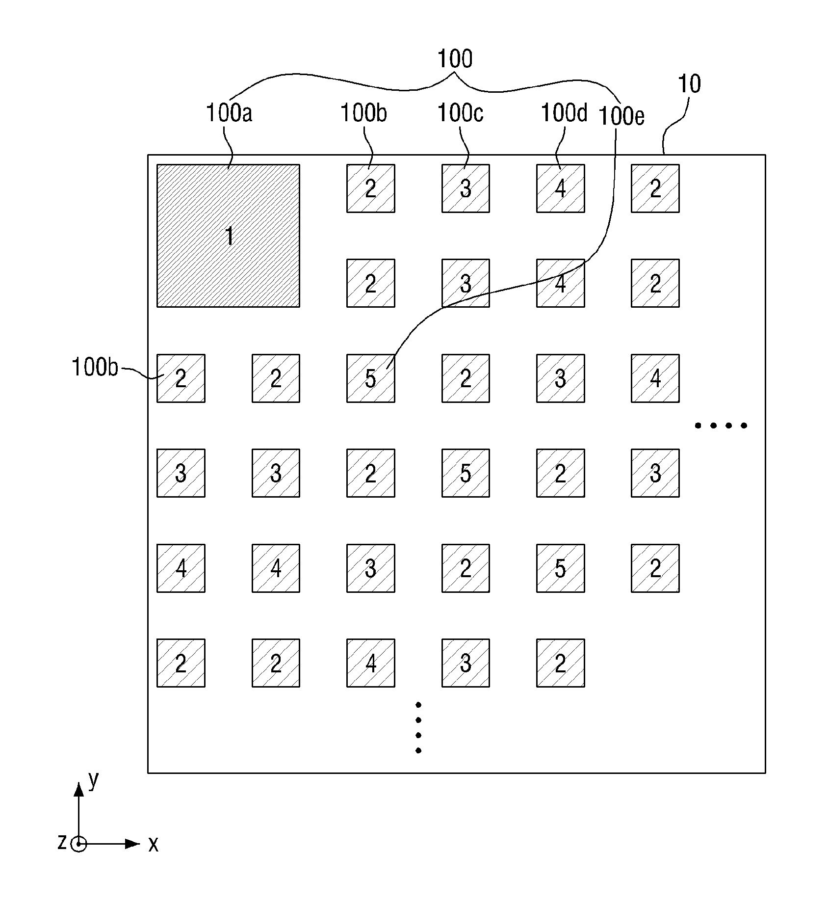
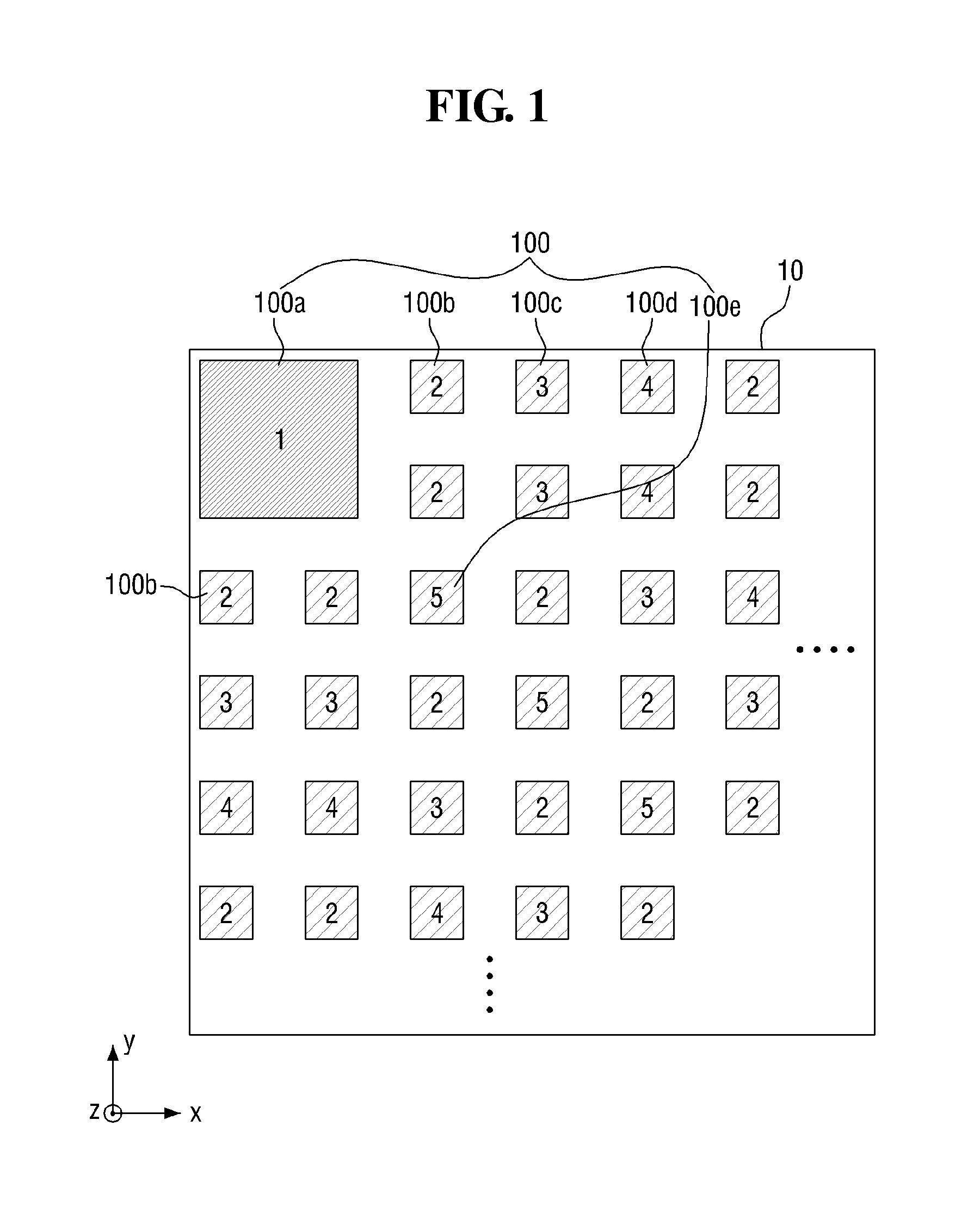
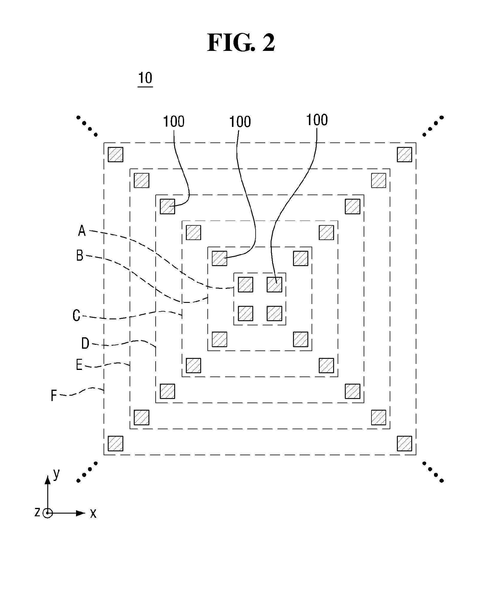
[0056]Hereinafter, a CPI test vehicle according to the inventive concept will be described in detail with reference to FIGS. 2 and 3.

[0057]The CPI test vehicle has sections A to F spaced from a neutral point, in this case the geometric center of the chip 10 as viewed in plan; thus, the sections A to F are arrayed along the diagonal from the center of the chip. Each of the sections A to F contains a plurality of sub-regions 100 with the sub-regions 100 in each section A to F disposed the same distance to the neutral point (DNP). In this example, each section A to F is rectangular and contains four sub-regions 100 at the respective corners of the section such that the four sub-regions 100 of each section A to F have the same DNP. That is, each of the sub-regions 100 of section A are spaced the same distance “a” from the center of the chip (FIG. 3), each of the sub-regions 100 of section B of the chip are spaced the same distance “b” from the center of the chip, etc., and the distances...

seventh embodiment

[0092]Hereinafter, a CPI test vehicle according to the inventive concept will be described with reference to FIG. 12.

[0093]FIG. 12 is a floor plan of chips for explaining the CPI test vehicle according to the seventh embodiment of the inventive concept.

[0094]Referring to FIG. 12, the CPI test vehicle according to the seventh embodiment of the inventive concept includes a plurality of chips 10a, 10b, 10c, 10d, 10e and 10f. A conventional floorplan has chips of different sizes by which a package is freely formed.

[0095]On the other hand, in the CPI test vehicle of the present embodiment, the chips 10a, 10b, 10c, 10d, 10e and 10f have the same shape and size. Further, in the CPI test vehicle of the present embodiment, each of the chips 10a, 10b, 10c, 10d, 10e and 10f may have a rectangular shape. Thus, adjacent ones of the chips 10a, 10b, 10c, 10d, 10e and 10f may be circumscribed within any of several different rectangles (two of which are shown in the example of FIG. 12 within the das...


PUM


Abstract

A chip to package interaction (CPI) test vehicle includes a chip including metal patterns contained in first and second sub-regions, respectively, and in which any one of the following comparable properties (a)˜(e) is the same among the first and second sub-regions, and another one of the properties (a)˜(e) is different among the first and second sub-regions: (a) size and shape of the sub-region, (b) metal density of the metal pattern, (c) type of the metal pattern, (d) distance between the sub-region and a center of the chip, (e) structure of the metal pattern.

Description

PRIORITY STATEMENT[0001]This application claims priority, and all the benefits accruing therefrom under 35 U.S.C. 119, from Korean Patent Application No. 10-2014-0026095 filed on Mar. 5, 2014 in the Korean Intellectual Property Office, the contents of which are hereby incorporated by reference in their entirety.BACKGROUND[0002]1. Technical Field[0003]The present inventive concept relates to a chip to package interaction (CPI) test vehicle and to a method for testing chip to package interaction using the same.[0004]2. Description of the Related Art[0005]A manufacturing technology for large scale integrated circuits (LSI) often includes the packaging of a chip comprising the LSI to a substrate having interconnections by which the LSI may be connected to an external device. In this technology, the chip to package interaction (CPI) is critical in realizing a high yield of reliable products. As LSI devices are scaled down, CPI failures, in which the chips do not operate normally, are inc...

Claims


Application Information

Patent Timeline
IPC IPC(8): G01R31/26
CPCG01R31/2607G01R31/2896
Inventor LEE, SANG-MANKANG, YOUNG-MINBANG, YONG-SEUNG
Owner SAMSUNG ELECTRONICS CO LTD
Why Eureka
Try Eureka