Semiconductor memory

a semiconductor memory and memory technology, applied in the field of semiconductor memory, can solve the problems of obstructing the practical use of the single-intersection memory cell array, increasing array noise during data reading, and reducing the access time and size of the chip including the semiconductor memory, so as to minimize the noise of the array during reading and maximize the margin

Inactive Publication Date: 2005-05-17
RENESAS TECH CORP
View PDF13 Cites 3 Cited by
  • Summary
  • Abstract
  • Description
  • Claims
  • Application Information

AI Technical Summary

Benefits of technology

[0018]Whenever external access is made to the semiconductor memory, the data registers are also accessed. When data items read from the data registers are written simultaneously in the memory cell array, the data items are encoded. When data items are read from the memory cells into the data registers, a flag is referenced in order to decode the data items. The encoders and encoding control circuit of the semiconductor memory are designed to perform these actions. Consequently, the array noise occurring during reading is minimized and the margin is maximized. The access time and size of the chip including the semiconductor memory are also minimized.

Problems solved by technology

However, compared with the dual-intersection memory cell array, the single-intersection memory cell array has a drawback that the array noise increases during data reading.
This obstructs practical use of the single-intersection memory cell array.
Moreover, even in the dual-intersection memory cell array, when a difference between capacitance levels of two parasitic capacitors formed between complementary bit lines and a word line gets so large that the noise cannot be canceled, the problem of increasing array noise persists.
If the amount of intelligence decreases because of an accompanying noise, the signal may be inverted incorrectly.
A similar noise occurs because of a plate that is a counter electrode of a capacitor included in a memory cell or a substrate of a transistor included in the memory cell.
If the number of bits received in sequence is small, the number of flag memory cells included in a chip increases and undesirably increases chip size.
Such determination takes a long time to make and undesirably increases the time required for the memory cycle.
Moreover, the criterion that the number of 1s occupies 25% or less or 75% or more used in the semiconductor memory having encoders of the related art is so complex that it undesirably increases the circuit scale and the area of a chip.

Method used


Image

  • Semiconductor memory
  • Semiconductor memory
  • Semiconductor memory

Examples


first exemplary embodiment

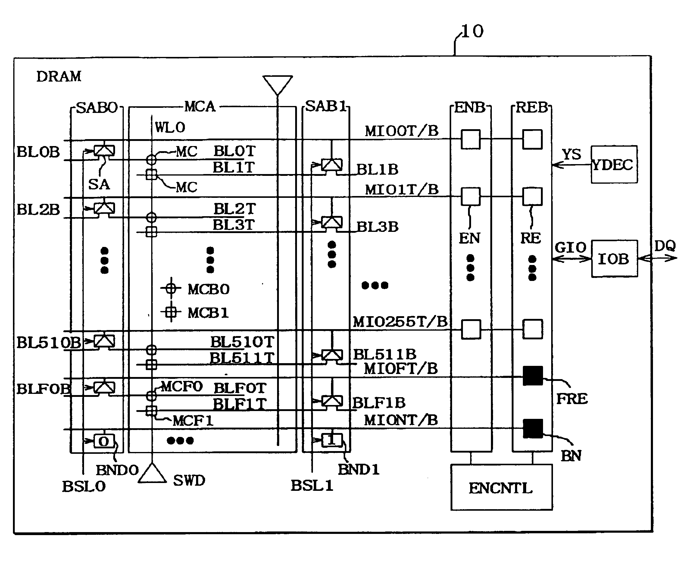
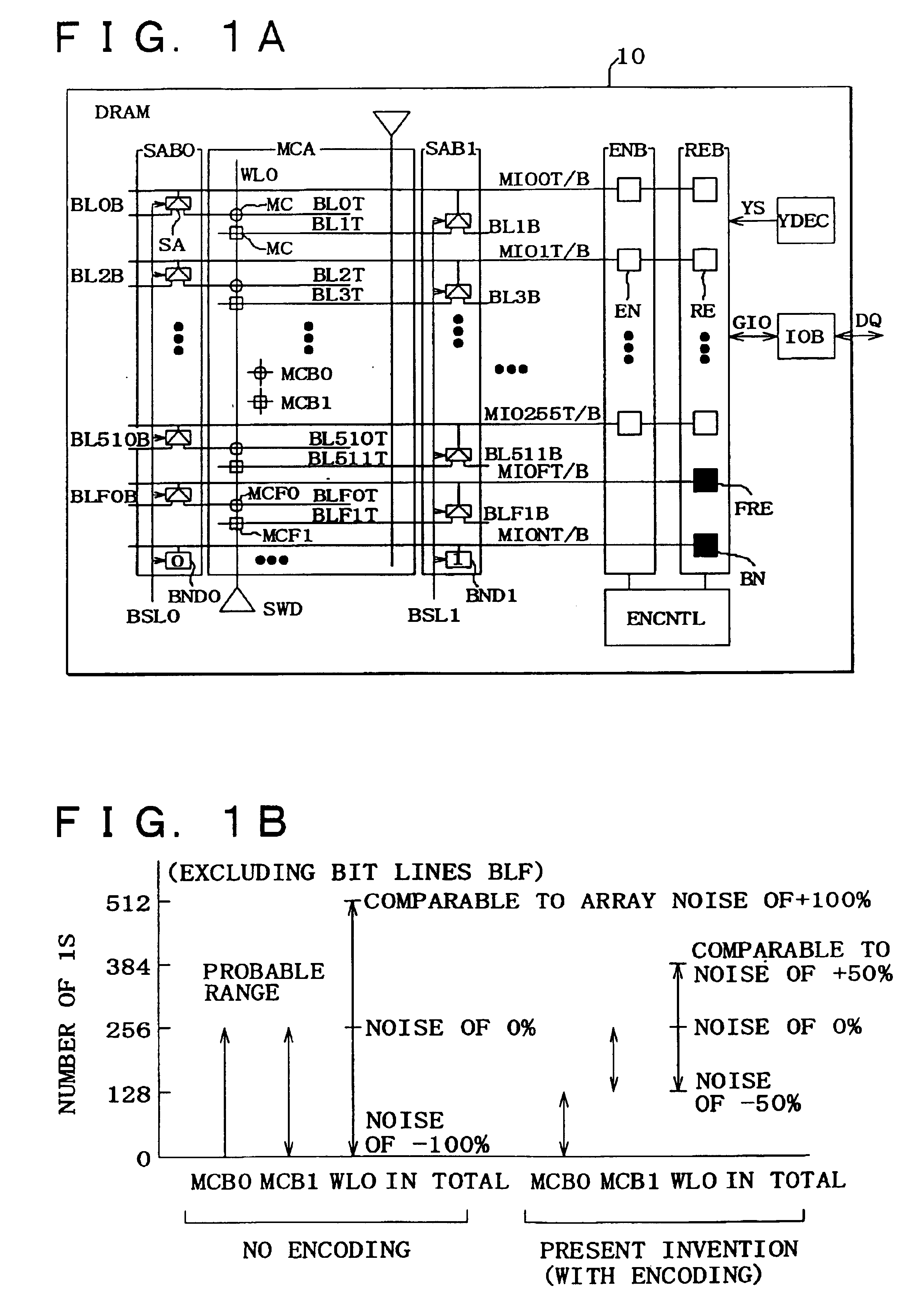
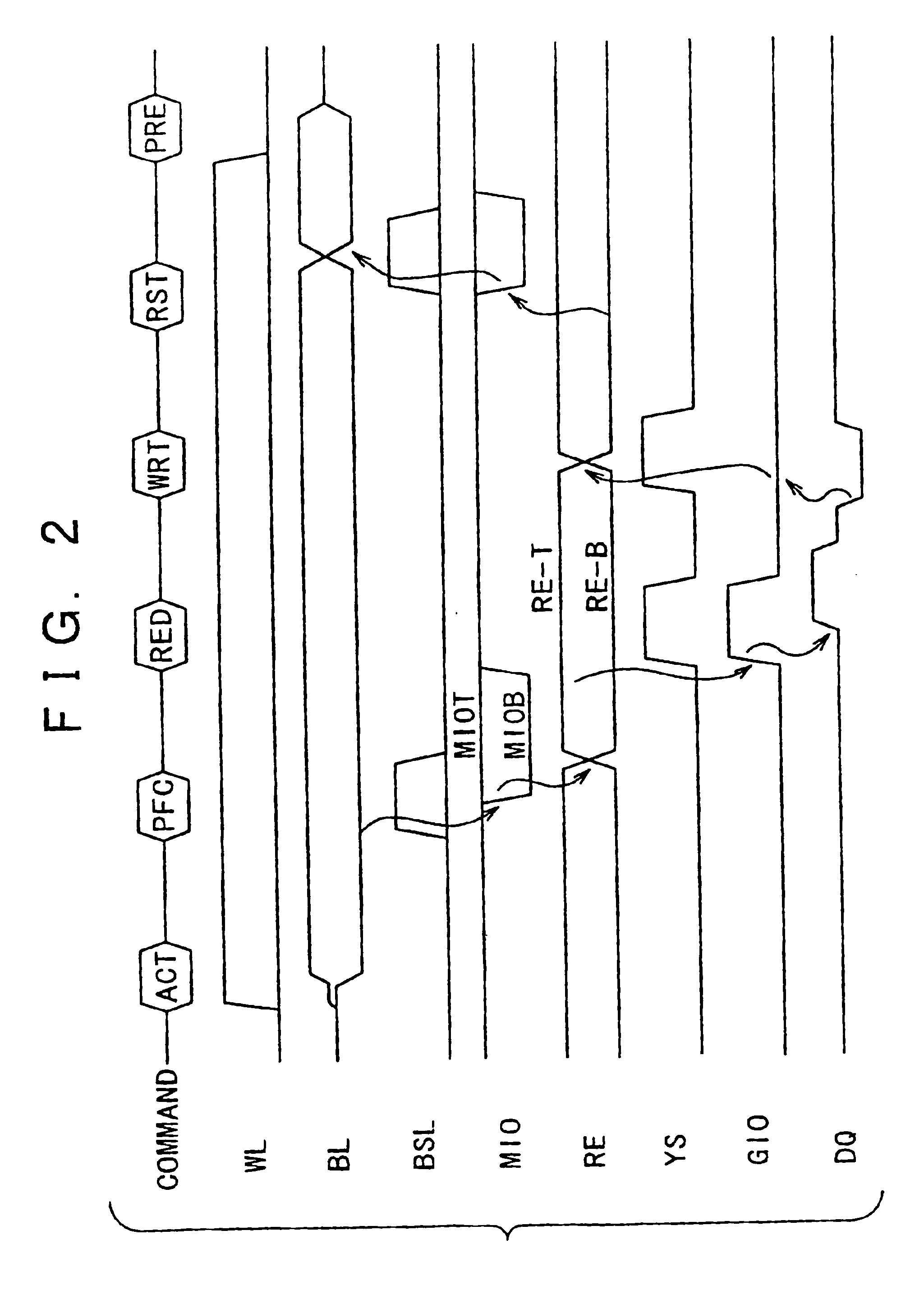
[0034]FIG. 1A shows the circuitry of a low-noise encoding DRAM of a semiconductor memory of a first preferred embodiment of the present invention. FIG. 2 shows the waveforms relevant to the functions performed therein. In the semiconductor chip incorporating the low-noise encoding DRAM 10 of the present invention, an Activate command ACT is issued when data items are to be read or written. The data items stored in memory cells MC constituting a memory cell array MCA are read and held in sense amplifiers SA belonging to sense amplifier banks SAB0 and SAB1.

[0035]After the pre-charging of the sense amplifiers SA is terminated, a sub-word driver SWD activates the word line WL0 so as to read data items from the memory cells MC onto bit lines BL0T, BL1T . . . BL510T, BL511T, etc. The sense amplifiers SA amplify the differences between weak signals developed on the bit lines and reference potentials on side-B bit lines BL0B, BL1B . . . BL510B. BL511B, etc., and hold the results.

[0036]As sh...

second exemplary embodiment

[0072]FIG. 7 shows an example of the circuitry of another preferred embodiment of the present invention comprising a register-incorporated DRAM. The actions to be performed in the DRAM of this preferred embodiment are described below. An address signal ADD is transmitted to an address buffer ADDBUF. A chip selecting signal / CS, a row address strobe signal / RAS, a column address strobe signal / CAS, and a writing enabling signal / WE are transmitted to a command decoder COMDEC. A clock CLK and a clock-enabling signal CKE are transmitted to a clock generator CLKGEN. The command decoder COMDEC decodes a received control signal and determines an operation mode by selecting any of a reading mode, a writing mode, and a pre-charging mode. A control logic LOGIC produces control signals required depending on the operation mode within a chip. A mode register MDREG holds a current operation mode. Reaister controller REGCNTL receives a sianal from address buffer ADDBUF and controls the register s...

third exemplary embodiment

[0077]FIG. 8 shows another preferred embodiment of the present invention comprising a multi-chip module MCP. A plurality of chips that are hard to be integrated into one chip, such as a DRAM chip 80, a flash memory chip 81, and a logic chip 82 are mounted on a silicon substrate 83, and interconnected using a silicon process. The number of connections is therefore much larger than the one on a normal printed-circuit board, but the area occupied by the mounted chips is reduced.

[0078]Consequently, the number of input / output pins formed on each chip can be increased. The DRAM chip 80 can transmit data items externally via a bi-directional buffer BDB over the main input / output lines MIO shown in FIG. 1. If the logic chip 82 includes the data register bank REB and encoder bank ENB, the DRAM chip 80 can be designed to have standard specifications. The specifications for the logic chip 82 can be modified. In this case, the DRAM chip 80 can be mass-produced since it can be adapted to work wi...


PUM


Abstract

A DRAM adopting a single-intersection memory cell array having randomly accessible data registers accessed whenever the chip is accessed externally. When data items recorded in the data registers are simultaneously written in the memory cell array, the data items are encoded. When data items are read from the memory cell array into the data registers, the data items are decoded. The margin is enhanced because array noise derived from reading is reduced. In addition, the access time of the DRAM is also reduced.

Description

[0001]This application is a Continuation of nonprovisional U.S. application Ser. No. 10 / 287,678 filed Nov. 5, 2002, U.S. Pat. No. 6,721,194. Priority is claimed based on U.S. application Ser. No. 10 / 287,678 filed Nov. 5, 2002, which claims the priority of Japanese appilcation 2001-338938 filed on Nov. 5, 2001.BACKGROUND OF THE INVENTION[0002]1. Field of the Invention[0003]The present invention relates to a semiconductor memory, and more particularly, to a dynamic random access memory (DRAM) whose margin can be expanded by minimizing noise occurring in a memory cell array comprising single-intersection memory cells.[0004]2. Description of the Related Art[0005]DRAMs are generally used to reduce the area of a chip and hence minimize the manufacturing costs thereof. FIG. 9A shows a single-intersection memory cell array having memory cells connected at all intersections of word lines WL (WL0, WL1, WL2) and bit lines BL (BL0B, BL0T, BL1B, BL1T, BL2B, BL2T). Compared with known dual-inters...

Claims


Application Information

Patent Timeline
Patent Type & Authority Patents(United States)
IPC IPC(8): G11C11/4096G11C7/10G11C11/409G11C11/407G11C11/401G11C11/404
CPCG11C5/025G11C7/02G11C7/1006G11C7/1051G11C7/1078G11C7/1087G11C11/405G11C11/4096G11C7/106G11C2207/107G11C11/407
Inventor SEKIGUCHI, TOMONORITAKEMURA, RIICHIROSAKATA, TAKESHIAYUKAWA, KAZUSHIGEKAWAHARA, TAKAYUKI
Owner RENESAS TECH CORP
Why Eureka
Try Eureka