Semiconductor device and method for operating the same

a technology of semiconductor devices and semiconductors, applied in the field of semiconductor devices, to achieve the effect of maximizing the input data margin

Active Publication Date: 2016-06-07
SK HYNIX INC
View PDF3 Cites 0 Cited by
  • Summary
  • Abstract
  • Description
  • Claims
  • Application Information

AI Technical Summary

Benefits of technology

[0012]Various embodiments are directed to a semiconductor device capable of adjusting offsets of a plurality of data buffers such that the data buffers have the same reference level, thereby maximizing the margin of input data, and a method for operating the same.

Problems solved by technology

In general, semiconductor circuits including differential amplifiers in data buffers have offsets which occur due to errors in design, the semiconductor fabrication process, packaging errors, or the external environment.

Method used


Image

  • Semiconductor device and method for operating the same
  • Semiconductor device and method for operating the same
  • Semiconductor device and method for operating the same

Examples


Embodiment Construction

[0030]Various embodiments will be described below in more detail with reference to the accompanying drawings. The present invention may, however, be embodied in different forms and should not be construed as limited to the embodiments set forth herein. Rather, these embodiments are provided so that this disclosure will be thorough and complete, and will fully convey the scope of the present invention to those skilled in the art. Throughout the disclosure, like reference numerals refer to like parts throughout the various figures and embodiments of the present invention.

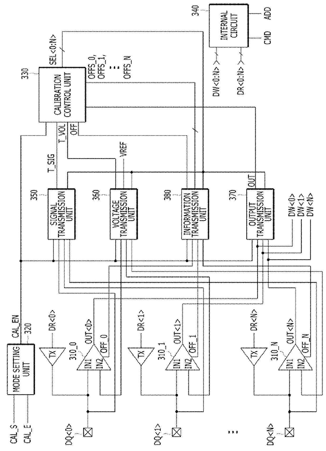
[0031]FIG. 3 is a block diagram illustrating a semiconductor device in accordance with an embodiment of the present invention.

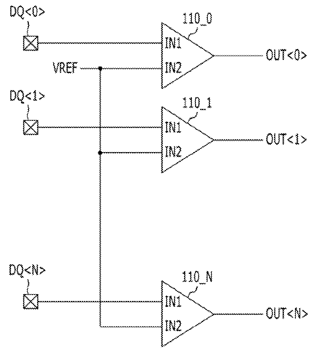
[0032]As illustrated in FIG. 3, the semiconductor device may include a plurality of data pads DQ, a plurality of data buffers 310_0 to 310_N, a mode setting unit 320, a calibration control unit 330, a plurality of transmitters TX, and an internal circuit 340. Furthermore, the semiconductor devi...


PUM


Abstract

A semiconductor device may include: a plurality of data pads; a plurality of data buffers each suitable for buffering a signal inputted through a first input node using a voltage inputted through a second input node, and outputting the buffered signal; and a calibration control unit suitable for generating a test signal in a calibration mode, adjusting the level of the test signal, receiving outputs of the plurality of data buffers while adjusting the level of the test signal, and adjusting offsets of the data buffers such that the logical values of the outputs of the data buffers transit when the test signal has a target level.

Description

CROSS-REFERENCE TO RELATED APPLICATIONS[0001]The present application claims priority of Korean Patent Application No. 10-2014-0074303, filed on Jun. 18, 2014, which is incorporated herein by reference in its entirety.BACKGROUND[0002]1. Field[0003]This patent document relates to a semiconductor device and a method for operating the same.[0004]2. Description of the Related Art[0005]FIG. 1 is a block diagram illustrating a plurality of data pads DQ<0:N> and a plurality of data buffers 110_0 to 110_N which are included in a semiconductor device. The plurality of data buffers 110_0 to 110_N may buffer data inputted to the corresponding data pads and output the buffered data as outputs OUT<0:N>.[0006]Each of the data buffers 110_0 to 110_N receives data from the corresponding data pad through a first input terminal IN1, receives a reference voltage VREF through a second input terminal IN2, buffers the data of the corresponding data pad using the reference voltage VREF, and out...

Claims


Application Information

Patent Timeline
Patent Type & Authority Patents(United States)
IPC IPC(8): G11C7/10G11C11/401G11C29/50G11C29/02
CPCG11C7/1084G11C7/1048G11C11/401G11C29/02G11C29/50G11C2207/105G11C2207/2254G11C7/10G11C7/12G11C29/12
Inventor SONG, CHOUNG-KI
Owner SK HYNIX INC
Why Eureka
Try Eureka