

Determining a cell state of a resistive memory cell
a resistive memory and cell state technology, applied in the field of determining the cell state of a resistive memory cell, can solve the problems of errors in retrieving stored data, difficulty in storing multiple resistance levels in a pcm cell, and difficulty in reading mlc cells, etc., to achieve faster readout of voltage-based cell state metrics, inherent slowness of current biasing, and fast readout schemes
- Summary
- Abstract
- Description
- Claims
- Application Information
AI Technical Summary
Benefits of technology
Problems solved by technology
Method used
Image

Examples
first embodiment
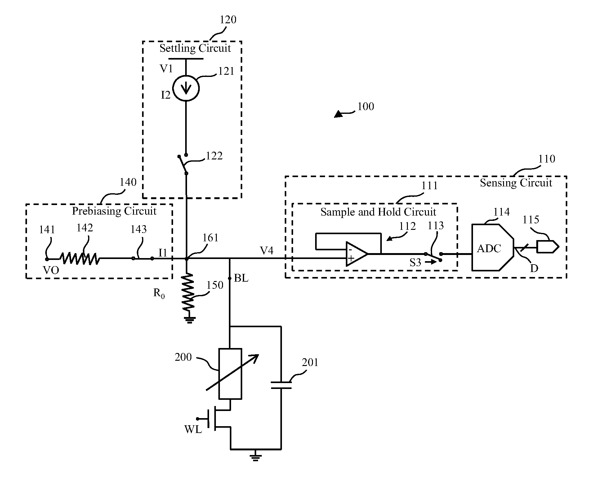
[0066]In FIG. 2, a device 100 for determining an actual cell state of a resistive memory cell 200 in a prebiasing mode is depicted.
[0067]The device 100 of FIG. 2 has a sensing circuit 110, a settling circuit 120, a prebiasing circuit 130 and a resistor 150. The resistor 150 is coupled in parallel to the resistive memory cell 200. For example, the resistive memory cell 200 is a PCM cell having a plurality M of programmable cell states.
[0068]The sensing circuit 110 is configured to sense a sensing voltage V4 of the resistive memory cell 200 and to output a resultant value D (e.g., a digital value D) in response to the sensing voltage V4. The sensing voltage V4, and therefore also the resultant value D, are indicative for the actual cell state.
[0069]The sensing circuit 110 includes a sample and hold circuit 111, an analog-to-digital converter (“ADC”) 114 and an output 115. The sample and hold circuit 111 includes a buffer 112 and a switch 113 controlled by control signal S3.
[0070]The s...
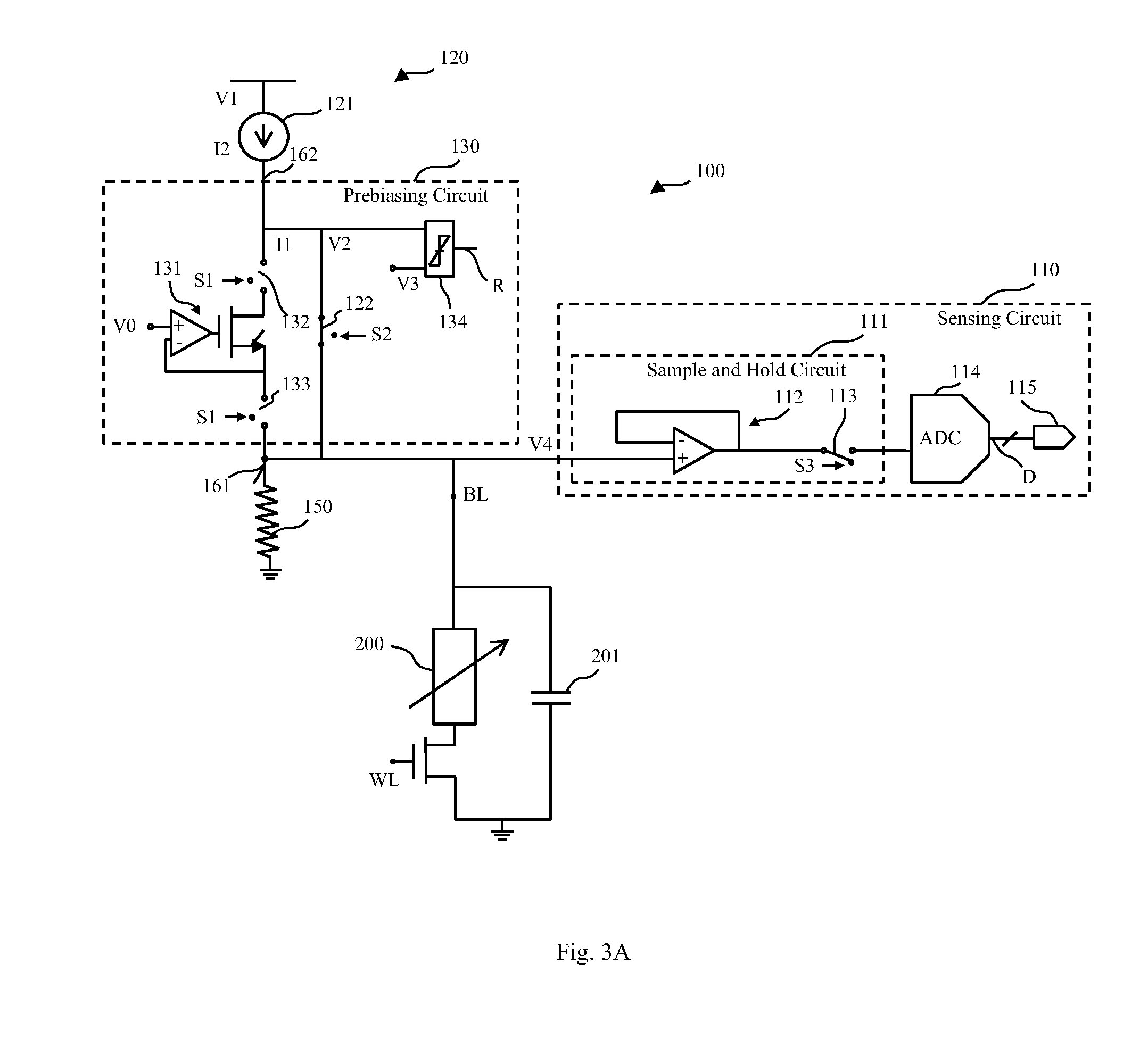
second embodiment
[0085]Further, FIGS. 5-7 show the device 100 in different operating modes.
[0086]FIG. 5 shows the device 100 in the prebiasing mode. In the prebiasing mode, the switch 122 is opened, the switch 143 is closed and the switch 113 is opened. In FIG. 5, the current flows from the voltage source 141 over the first node 161 to the bitline BL and therefore to the resistive memory cell 200. The current flow in FIG. 5 is shown by arrow A1.
[0087]Further, in the settling mode according to FIG. 6, the switch 143 is opened, the switch 122 is closed and the switch 113 is open. As a result, the current flows from the current mirror 121 to the resistive memory cell 200 over the first node 161 and the bitline BL. The current flow in FIG. 6 is shown by arrow A2.
[0088]In FIG. 7, the device 100 is in a sampling mode. In the sampling mode, the switch 143 is opened, the switch 122 is closed and the switch 113 is closed. The controller controls the sampling by the third control signal S3 applied to switch 1...
PUM
 Abstract
Description
Claims
Application Information