Display device and electronic device

a display device and electronic technology, applied in the field of display devices, can solve the problems of imposing limitations on the shape of the display region and significant limitations in the housing design, and achieve the effects of reducing frame width, minimizing the external shape of the display device, and high degree of flexibility of the display region

Inactive Publication Date: 2015-12-24
SEMICON ENERGY LAB CO LTD
View PDF5 Cites 12 Cited by
  • Summary
  • Abstract
  • Description
  • Claims
  • Application Information

AI Technical Summary

Benefits of technology

[0015]Regardless of whether a display region of a display device is non-rectangular or rectangular, the display region is expected to be maximized so that the visibility of the display device can be increased by reducing the frame width, for example. The display device needs to include an input terminal region for inputting an external signal, such as an image signal, into the display device. The input terminal region is usually provided in a frame region outside the display region and thus requires a frame region with a certain width outside the display region, which have prevented the maximization of the display region.
[0016]In view of the above problems, an object of one embodiment of the present invention is to provide a display device having a reduced frame width and a shape that is not significantly different from the shape of a display region included in the display device regardless of whether the display region has a rectangular or non-rectangular shape. Another object is to provide a display device in which a display region can be maximized. Another object is to provide a display device that can be easily downsized. Another object of one embodiment of the present invention is to provide a display device having a novel structure.
[0021]According to one embodiment of the present invention, a high degree of flexibility of the shape of a display region and minimization of the external shape of a display device with a reduced frame width can be achieved; thus, a display device with less limitation of design flexibility can be provided.
[0022]According to one embodiment of the present invention, a display device having a reduced frame width and a shape that is not significantly different from the shape of a display region included in the display device can be provided regardless of whether the display region has a rectangular or non-rectangular shape. According to one embodiment of the present invention, a display device in which a display region can be maximized can be provided. A display device that can be easily downsized can be provided. According to one embodiment of the present invention, a novel display device can be provided.

Problems solved by technology

According to such methods, although a display region can have a non-rectangular shape, housing design is significantly limited.
However, these modes require at least one vertex between a data driver (source driver) and a gate driver, which imposes limitations on the shape of the display region.

Method used


Image

  • Display device and electronic device
  • Display device and electronic device
  • Display device and electronic device

Examples


embodiment 1

[0084]Examples of a structure of a display device 100 and a manufacturing method thereof according to one embodiment of the present invention are described with reference to drawings.

example 1

[Structure Example 1 of Display Device]

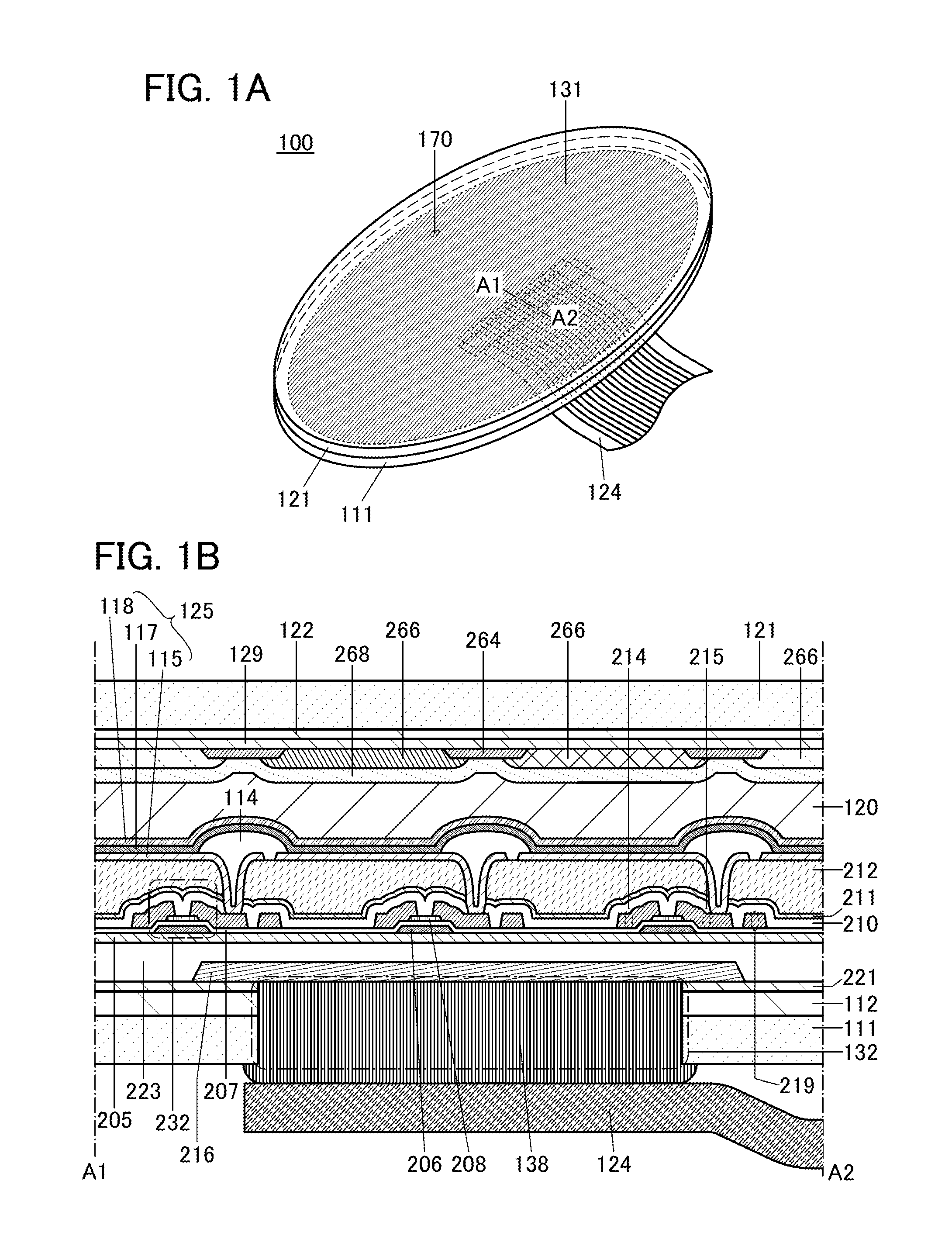
[0085]FIG. 1A is a perspective view of the display device 100 to which an external electrode 124 is connected. The external shape of the display device 100 illustrated in FIG. 1A is a non-rectangular shape. The display device 100 includes a display region 131 that has a non-rectangular shape. FIG. 1B is a cross-sectional view taken along the dash-dot line A1-A2 in FIG. 1A. The display device 100 disclosed in this specification is a display device in which a light-emitting element is used as a display element. As the display device 100 of one embodiment of the present invention, a display device having a top-emission structure is described as an example.

[0086]The display device 100 described in this embodiment includes the display region 131. The display device 100 also includes a terminal electrode 216 and a light-emitting element 125 including an electrode 115, an EL layer 117, and an electrode 118. A plurality of light-emitting elements 125 a...

example 2

[Structure Example 2 of Display Device]

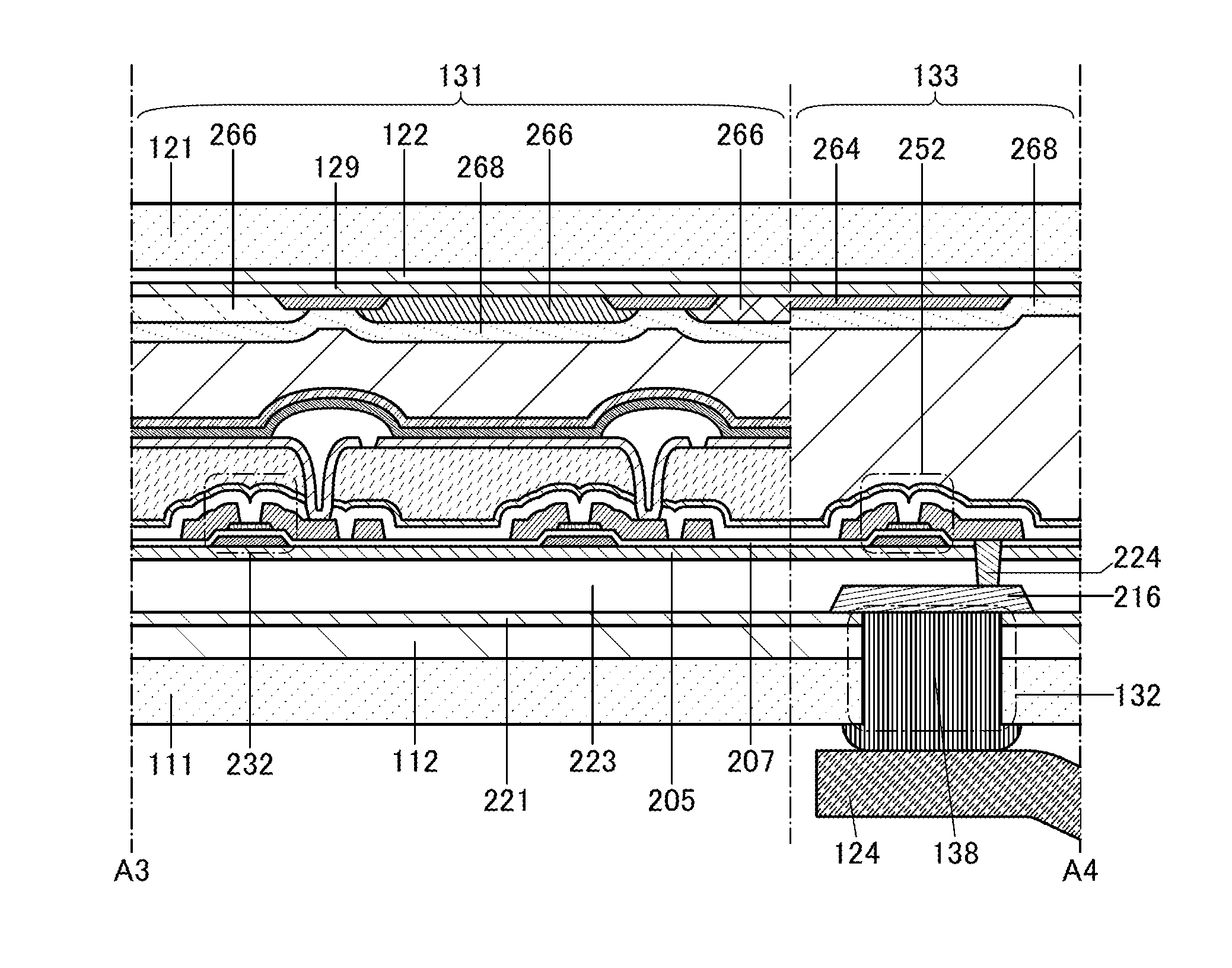
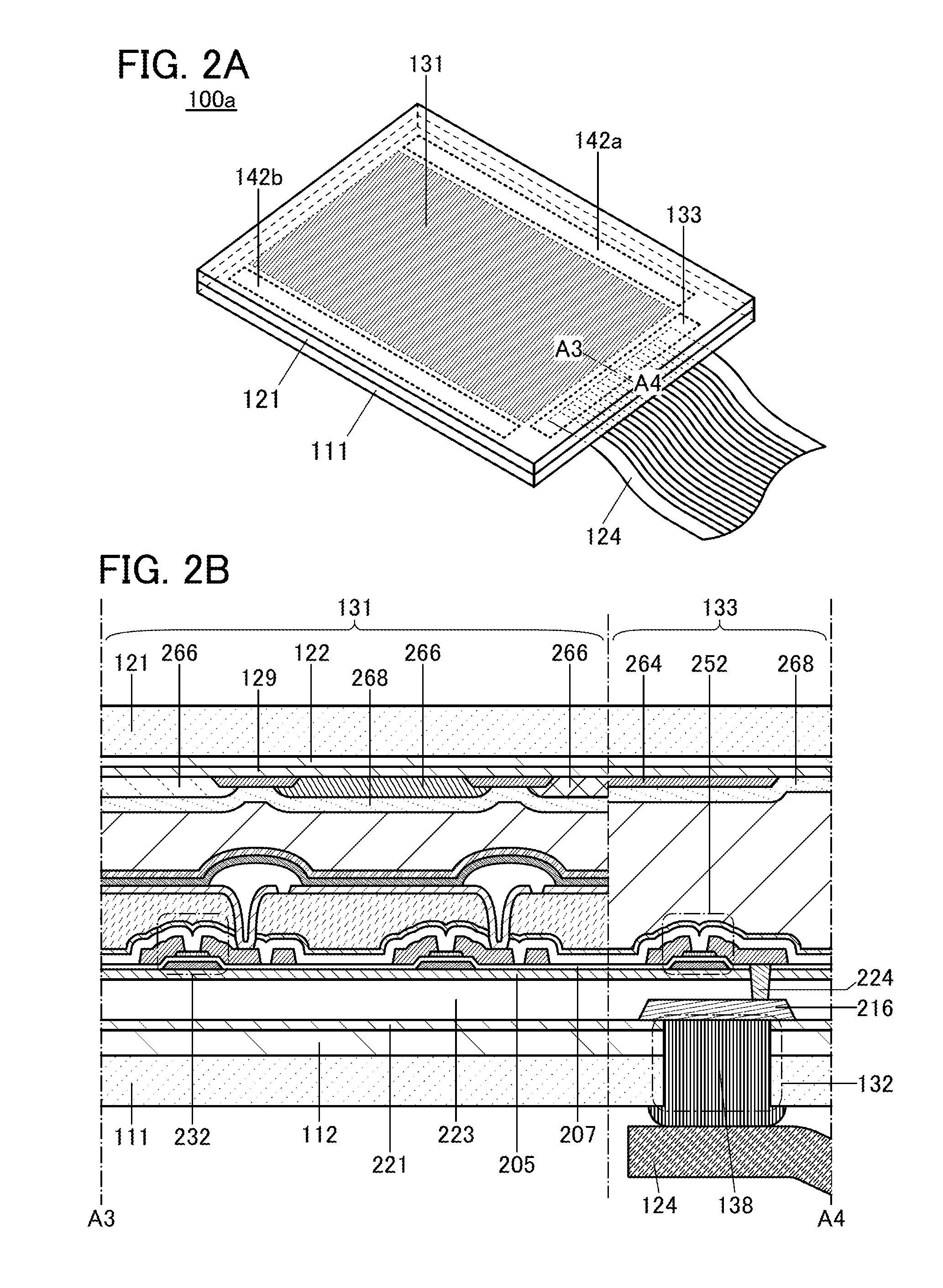
[0098]FIG. 2A illustrates the display device 100a having a rectangular external shape. FIG. 2A is a perspective view of the display device 100a having a rectangular shape to which the external electrode 124 is connected. FIG. 2B is a cross-sectional view taken along the dash-dot line A3-A4 in FIG. 2A. Note that components identical with those of the display device 100 illustrated in FIG. 1A are not described here.

[0099]The display device 100a illustrated in FIG. 2A includes the display region 131 having a rectangular shape. Outside the display region 131, a driver circuit 133, a driver circuit 142a, and a driver circuit 142b are provided. Note that in this specification and the like, one or more of the driver circuits 133, 142a, and 142b may be simply referred to as a driver circuit or a peripheral driver circuit.

[0100]The driver circuits 133, 142a, and 142b each include a plurality of transistors 252. The driver circuits 133, 142a, and 142b ea...


PUM


Abstract

A display device having a reduced frame width and a shape that is not significantly different from the shape of a display region is provided even in the case where the display region is non-rectangular. The display device includes a display region and a terminal electrode. The terminal electrode overlaps with the display region and is electrically connected to an external electrode through the non-display side of the display region.

Description

TECHNICAL FIELD[0001]The present invention relates to a display device. The present invention also relates to a method of manufacturing the display device.[0002]One embodiment of the present invention is not limited to the above technical field.[0003]The technical field of one embodiment of the invention disclosed in this specification and the like relates to an object, a method, or a manufacturing method. In addition, one embodiment of the present invention relates to a process, a machine, manufacture, or a composition of matter.[0004]The term display device refers to a device including a display element. The display device may include a driver circuit driving a plurality of pixels, a control circuit, a power supply circuit, a signal generation circuit, or the like. The term display device may refer to, for example, a module to which a connector such as a flexible printed circuit (FPC), tape automated bonding (TAB) tape, or a tape carrier package (TCP) is attached, a module in whic...

Claims


Application Information

Patent Timeline
Patent Type & Authority Applications(United States)
IPC IPC(8): H01L27/32H01L51/52
CPCH01L27/322H01L27/323H01L2251/5338H01L2251/5315H01L51/003H01L27/3276H10K59/38H10K59/40H10K71/80H10K59/131H10K2102/3026H10K2102/311G02F1/1343G06F3/041G06F2203/04103G06F2203/04102
Inventor YAMAZAKI, SHUNPEI
Owner SEMICON ENERGY LAB CO LTD
Why Eureka
Try Eureka