Display device and electronic device

a technology of electronic devices and display regions, which is applied in the direction of semiconductor devices, instruments, electrical devices, etc., can solve the problems of imposing limitations on serious limitations on the design of the housing, and achieves a high degree of flexibility of the shape of the display region, less limitation of design flexibility, and reduced frame width

Inactive Publication Date: 2019-02-12
SEMICON ENERGY LAB CO LTD
View PDF41 Cites 6 Cited by
  • Summary
  • Abstract
  • Description
  • Claims
  • Application Information

AI Technical Summary

Benefits of technology

[0015]Regardless of whether a display region of a display device is non-rectangular or rectangular, the display region is expected to be maximized so that the visibility of the display device can be increased by reducing the bezel width, for example. The display device needs to include an input terminal region for inputting an external signal, such as an image signal, into the display device. The input terminal region is usually provided in a frame region outside the display region and thus requires a frame region with a certain width outside the display region, which have prevented the maximization of the display region.
[0016]In view of the problems, an object of one embodiment of the present invention is to provide a display device having a reduced frame width without a significant alteration in the shape of a display region regardless of whether the shape is rectangular or non-rectangular. Another object is to provide a display device in which a display region can be maximized. Another object is to provide a novel display device.
[0022]According to one embodiment of the present invention, a high degree of flexibility of the shape of a display region and minimization of the outside shape of a display device with a reduced frame width can be achieved; thus, a display device with less limitation of design flexibility can be provided.
[0023]According to one embodiment of the present invention, a display device having a reduced frame width without a significant alteration in the shape of a display region regardless of whether the shape is rectangular or non-rectangular can be provided. According to one embodiment of the present invention, a display device in which a display region can be maximized can be provided. According to one embodiment of the present invention, a novel display device can be provided.

Problems solved by technology

In the case of such a method, limitation of housing design becomes serious even if the display region can have a non-rectangular shape.
However, these modes require at least one vertex along the shape of the display region between a data driver (source driver) and a gate driver, which imposes limitations on the shape of the display region.

Method used


Image

  • Display device and electronic device
  • Display device and electronic device
  • Display device and electronic device

Examples


embodiment 1

[0097]Examples of a structure of a display device 100 and a manufacturing method thereof according to one embodiment of the present invention are described with reference to drawings.

[Structure Example of Display Device]

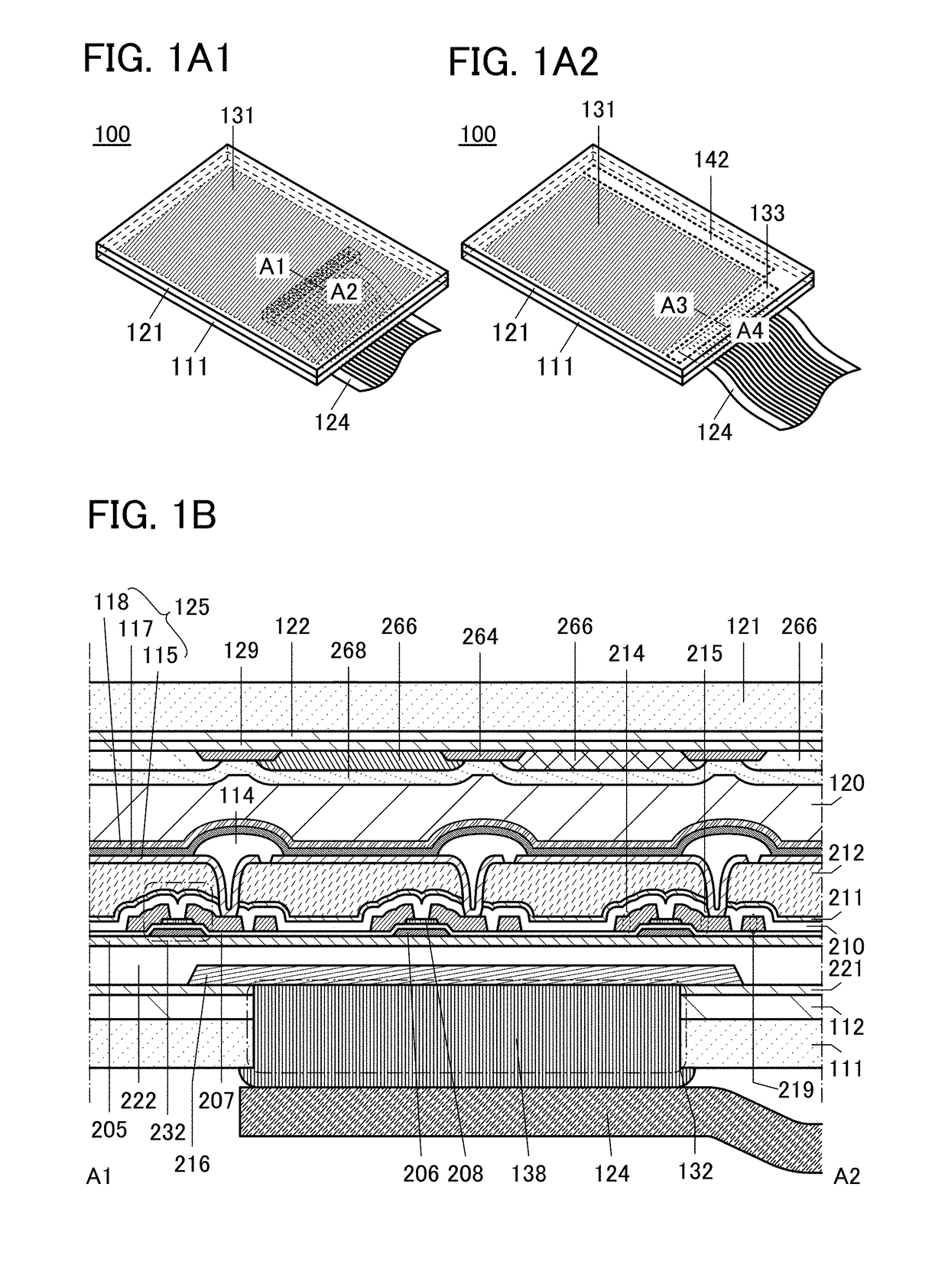
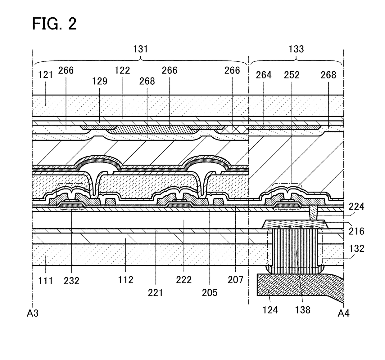
[0098]FIG. 1A1 is a perspective view of the display device 100 to which an external electrode 124 is connected. FIG. 1B is a cross-sectional view taken along the dash-dot line A1-A2 in FIG. 1A1. The display device 100 disclosed in this specification is a display device in which a light-emitting element is used as a display element. As the display device 100 of one embodiment of the present invention, a display device having a top-emission structure is described as an example.

[0099]The display device 100 described in this embodiment includes the display region 131. The display device 100 also includes a terminal electrode 216 and a light-emitting element 125 including an electrode 115, an EL layer 117, and an electrode 118. A plurality of light-emitting elements 125 a...

embodiment 2

[0219]In this embodiment, a specific structure example of the display device 100 is described with reference to FIGS. 15A to 15C. FIG. 15A is a block diagram of a configuration example of the display device 100.

[0220]FIG. 15A illustrates the display region 231 and the driver circuits 142a, 142b, and 133. The display region 231 in FIG. 15A corresponds to the display region 131 of the display device 100. The driver circuits 133, 142a, and 142b may be provided inside or outside the display device 100. Note that the driver circuits 142a, 142b, and 133 are collectively referred to as a driver circuit or a peripheral driver circuit in some cases.

[0221]The driver circuits 142a and 142b can function as, for example, scan line driver circuits. The driver circuit 133 can function as, for example, a signal line driver circuit. Note that one of the driver circuits 142a and 142b may be omitted. Alternatively, some sort of circuit facing the driver circuit 133 with the display region 231 provided...

embodiment 3

[0251]In this embodiment, an example of a transistor which can be used instead of the transistor 232 described in the above embodiments is described with reference to drawings. A transistor disclosed in this specification and the like can be applied to the transistors 431, 434, and the like.

[0252]The display device 100 of one embodiment of the present invention can be fabricated by using a transistor with any of various structures, such as a bottom-gate transistor, a top-gate transistor, or the like. Therefore, a material for a semiconductor layer or the structure of a transistor can be easily changed depending on the existing production line.

[Bottom-Gate Transistor]

[0253]FIG. 16A1 is a cross-sectional view of a transistor 410 that is a channel-protective transistor, which is a type of bottom-gate transistor. In FIG. 16A1, the transistor 410 is formed over a substrate 271. The transistor 410 includes an electrode 246 over the substrate 271 with an insulating layer 272 provided there...


PUM


Abstract

Provided is a display device whose display region can be maximized. The display device includes the display region and a terminal electrode. The terminal electrode overlaps with the display region and is electrically connected to an external electrode on a non-display surface of the display region.

Description

BACKGROUND OF THE INVENTION[0001]1. Field of the Invention[0002]One embodiment of the present invention relates to a transistor, a semiconductor device, and a manufacturing method thereof.[0003]Note that one embodiment of the present invention is not limited to the above technical field. The technical field of one embodiment of the invention disclosed in this specification and the like relates to an object, a method, or a manufacturing method. In addition, one embodiment of the present invention relates to a process, a machine, manufacture, or a composition of matter.[0004]In this specification and the like, a semiconductor device generally means a device that can function by utilizing semiconductor characteristics. A display device (e.g., a liquid crystal display device and a light-emitting display device), a lighting device, an electro-optical device, a power storage device, a memory device, a semiconductor circuit, an imaging device, an electronic device, and the like may include...

Claims


Application Information

Patent Timeline
Patent Type & Authority Patents(United States)
IPC IPC(8): G09G3/20H01L27/12
CPCG09G3/20H01L27/1225G09G3/035
Inventor YAMAZAKI, SHUNPEI
Owner SEMICON ENERGY LAB CO LTD
Why Eureka
Try Eureka