Substrate, display device, and method for manufacturing alignment film

Inactive Publication Date: 2016-01-21
TCL CHINA STAR OPTOELECTRONICS TECH CO LTD
View PDF7 Cites 0 Cited by
  • Summary
  • Abstract
  • Description
  • Claims
  • Application Information

AI Technical Summary

Benefits of technology

[0006]The objective of the present disclosure is to provide a substrate, a display device, and a method for manufacturing an alignment film, so as to solve the t

Problems solved by technology

Difference of feedthrough at different locations of the liquid cry

Method used


Image

  • Substrate, display device, and method for manufacturing alignment film
  • Substrate, display device, and method for manufacturing alignment film
  • Substrate, display device, and method for manufacturing alignment film

Examples


example 1

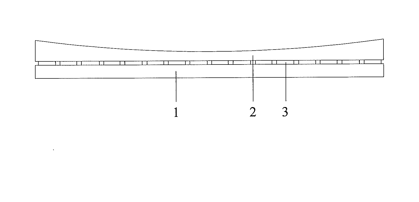
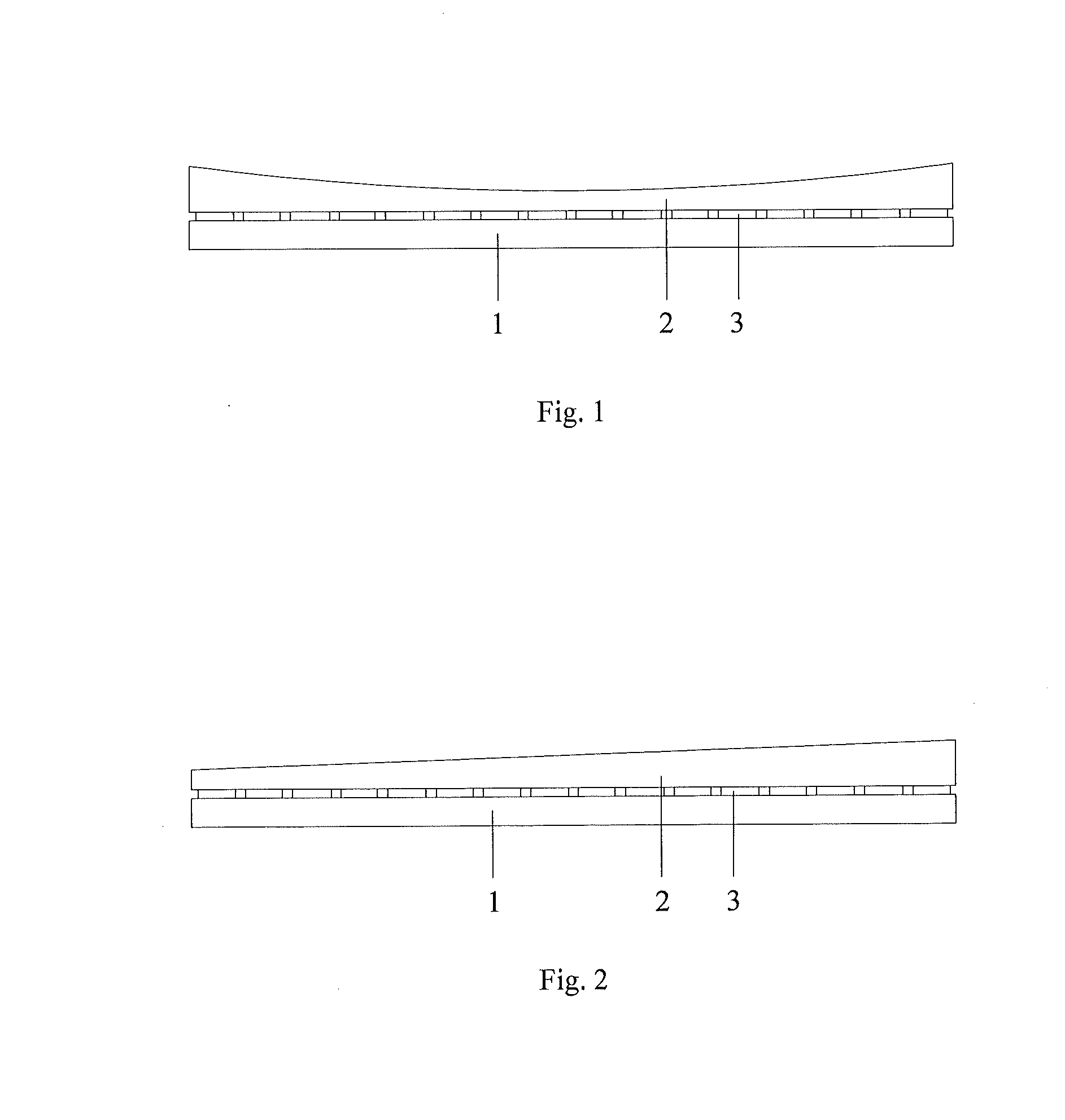
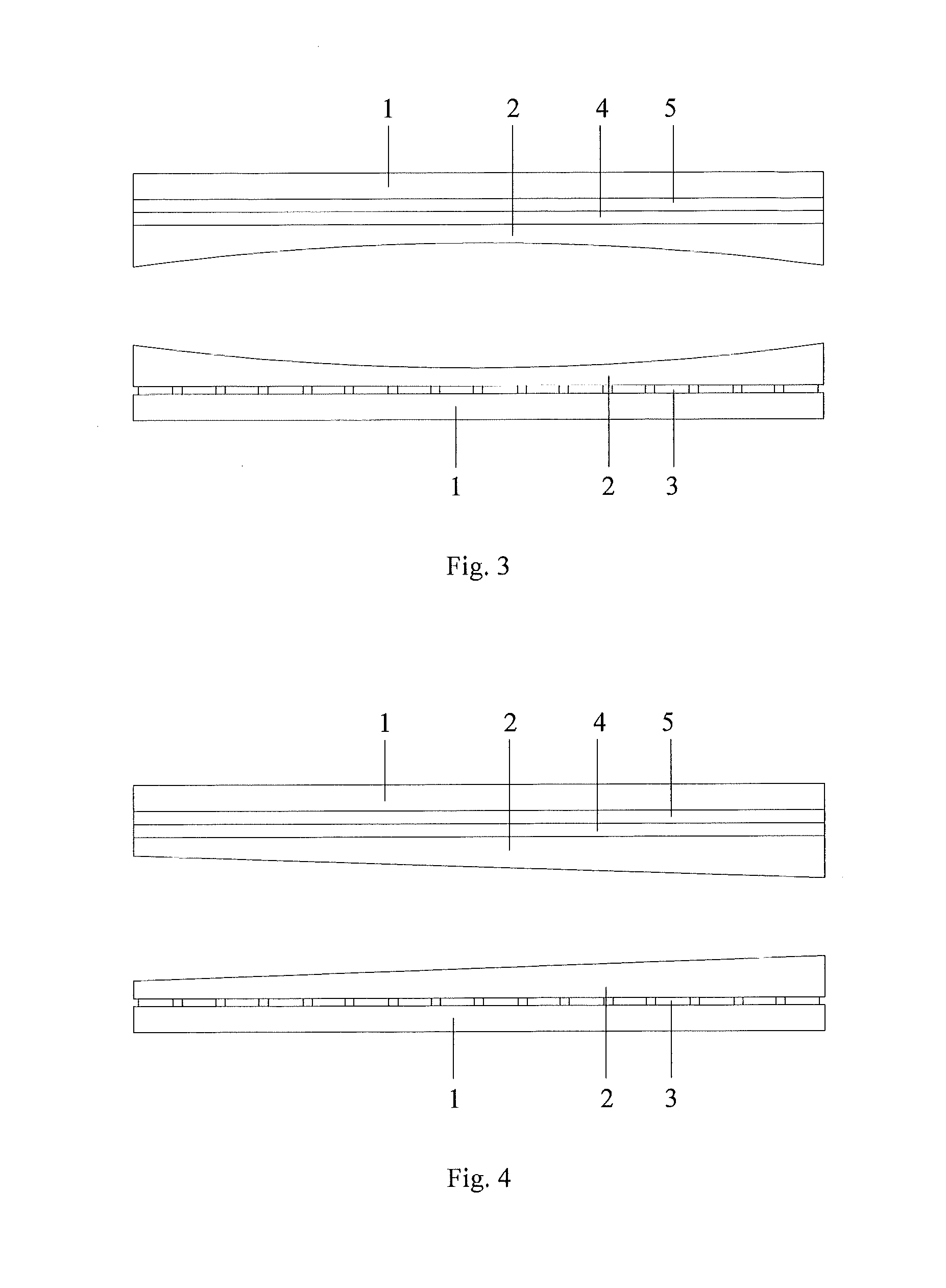
[0036]The substrate provided by the present example can be an array substrate, or a color filter substrate. As shown in FIG. 1, the present example is illustrated with an array substrate. The array substrate comprises a glass base 1, and an alignment film 2 formed on the glass base 1. The array substrate further comprises a thin film transistor (not shown) and a pixel electrode 3 disposed between the glass base 1 and the alignment film 2. If the substrate is embodied as a color filter substrate, a color filter layer and a common electrode are arranged between the glass base and the alignment film.

[0037]The array substrate provided by the present example can be used in a bi-directional driven liquid crystal display device. The thickness of the alignment film 2 in the array substrate, measured along a lateral direction, gradually becomes thinner from both ends of the alignment film 2 to the center thereof. Therefore, in a liquid crystal panel formed with this array substrate, the thic...

example 2

[0052]Example 2 is substantially the same as example 1. The difference of example 2 from example 1 is that the substrate according to this example can be used in a unidirectional driven liquid crystal display device. The substrate can be an array substrate comprising a glass base, an alignment film, and a thin film transistor and a pixel electrode disposed between the glass base and the alignment film, etc. The substrate can also be a color filter substrate comprising a glass base, an alignment film, and a color filter layer and a common electrode disposed between the glass base and the alignment film, etc.

[0053]The array substrate or color filter substrate according to this example is different from that of example 1 in that the thickness of the alignment film thereof measured along a lateral direction gradually becomes thinner from one end of the alignment film to the other end thereof. Thus, in a unidirectional driven liquid crystal panel formed with this array substrate or color...


PUM


Abstract

In the technical field of display, a substrate, a display device and a method for manufacturing an alignment film are disclosed. The present disclosure can solve the technical problem of image sticking of the liquid crystal display caused by the difference of feedthrough at different locations of the liquid crystal display device. The substrate of the present disclosure comprises a glass base and an alignment film formed on the glass base. The thickness of the alignment film measured along a lateral direction gradually becomes thinner from both ends of the alignment film to the center thereof, and/or the thickness of the alignment film measured along a longitudinal direction gradually becomes thinner from one end of the alignment film to the other end thereof. The present disclosure can be applied to display devices, such as liquid crystal television, liquid crystal display, mobile phone, and PC tablet, etc.

Description

[0001]The present application claims benefit of Chinese patent application CN 201410348811.0, entitled “SUBSTRATE, DISPLAY DEVICE, AND METHOD FOR MANUFACTURING ALIGNMENT FILM” and filed on Jul. 21, 2014, which is incorporated herein by reference.TECHNICAL FIELD [0002]The present disclosure relates to the technical field of display, and in particular, to a substrate, a display device, and a method for manufacturing an alignment film.TECHNICAL BACKGROUND [0003]As display technology develops, a planar substrate has been commonly used in liquid crystal display device.[0004]In a liquid crystal display device having various display modes, image sticking would more or less occur. That is, when changing a static picture after it is displayed over a prolonged period of time, a ghost image from the previous picture would be left behind. A main reason for image sticking is the difference of feedthrough at different locations of the liquid crystal display device, i.e., voltage drops produced by...

Claims


Application Information

Patent Timeline
IPC IPC(8): G02F1/1337B05D1/02G02F1/1335G02F1/1368H01L27/12
CPCG02F1/1337G02F1/133512G02F2001/133397H01L27/1214B05D1/02G02F1/1368H01L27/1218G02F2201/121G02F1/133397G02F1/133776G02F1/13606G02F1/133723G02F1/133711
Inventor CHEN, CAIQIN
Owner TCL CHINA STAR OPTOELECTRONICS TECH CO LTD
Why Eureka
Try Eureka