Eureka AIR delivers breakthrough ideas for toughest innovation challenges, trusted by R&D personnel around the world.

T-shaped fin isolation region and methods of fabrication

Inactive Publication Date: 2016-04-21
GLOBALFOUNDRIES INC
View PDF0 Cites 19 Cited by
  • Summary
  • Abstract
  • Description
  • Claims
  • Application Information

AI Technical Summary

Benefits of technology

The patent text describes a new method and device that provide an isolation feature within a fin structure. This method includes adding an isolation material to the fin structure, which includes a T-shaped region that extends into the fin structure and overlies it. This T-shaped region separates two different circuit elements supported by the fin structure. The technical effect of this invention is better electrical and / or signal isolation between different circuit elements, which improves the performance and reliability of the semiconductor device.

Problems solved by technology

This desire for large scale integration has led to a continued shrinking of circuit dimensions and component features.

Method used


Image

  • T-shaped fin isolation region and methods of fabrication
  • T-shaped fin isolation region and methods of fabrication
  • T-shaped fin isolation region and methods of fabrication

Examples


Embodiment Construction

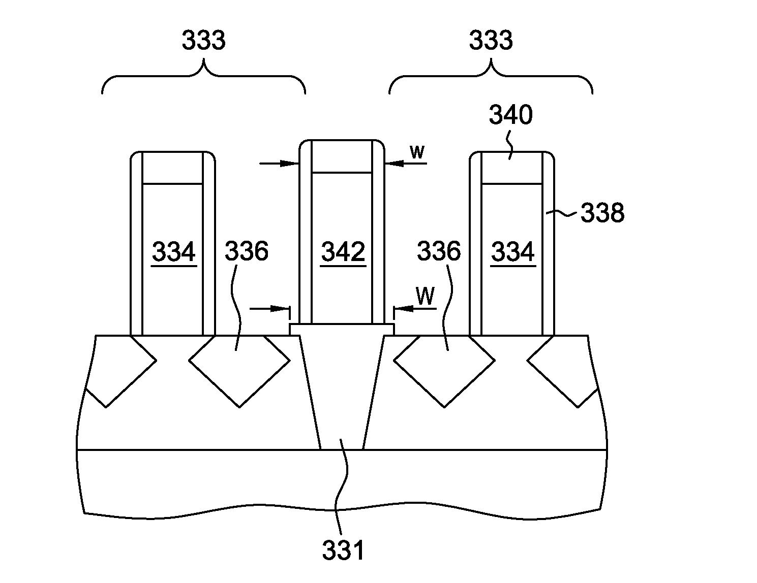
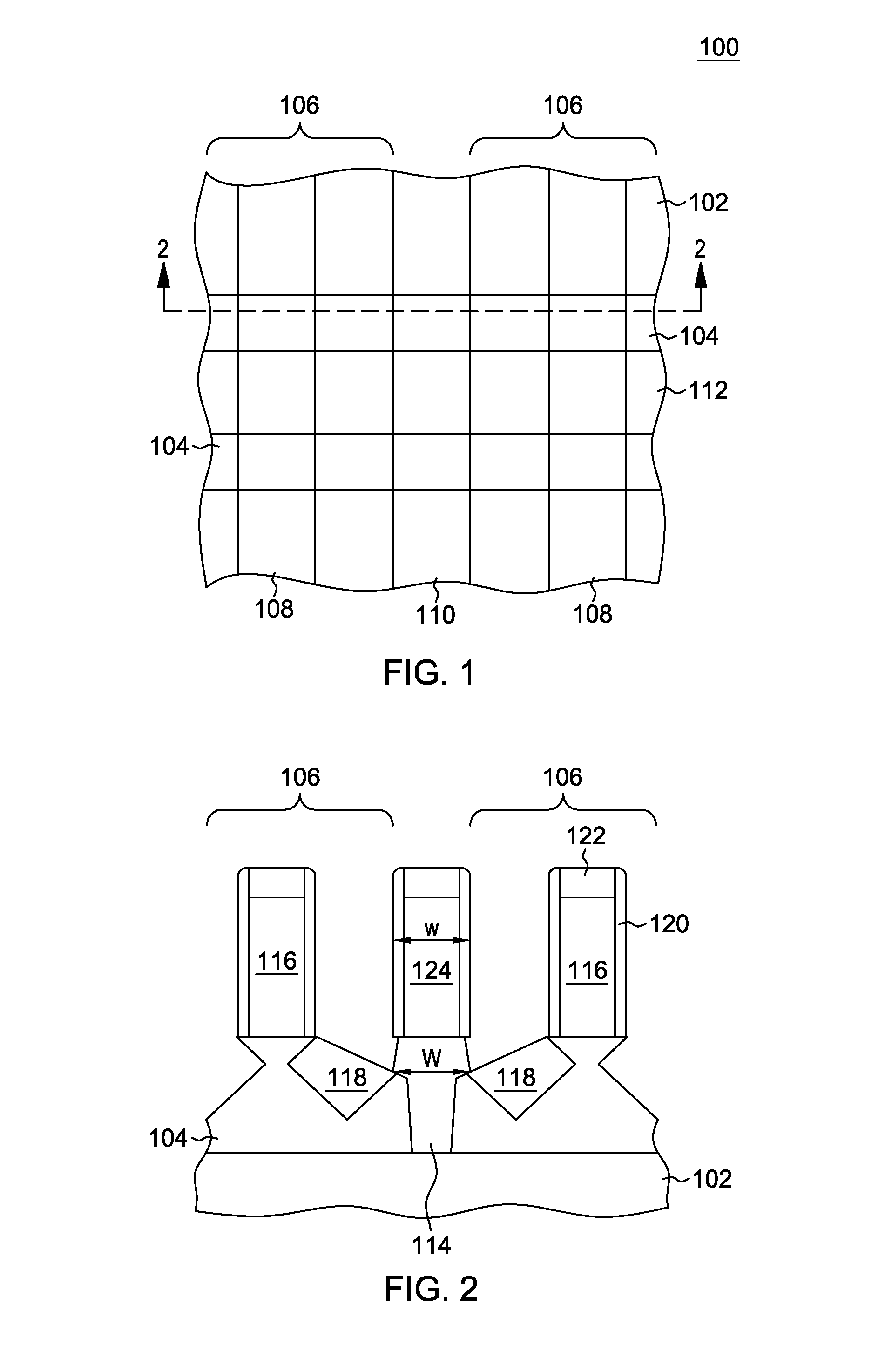
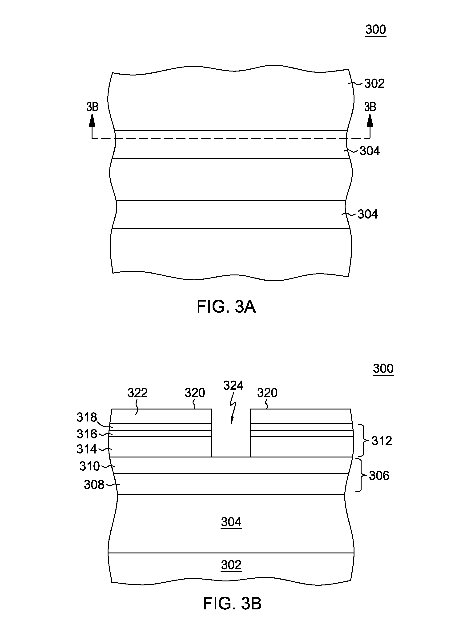
[0021]Aspects of the present invention and certain features, advantages, and details thereof, are explained more fully below with reference to the non-limiting embodiments illustrated in the accompanying drawings. Descriptions of well-known materials, fabrication tools, processing techniques, etc., are omitted so as to not unnecessarily obscure the invention in detail. It should be understood, however, that the detailed description and the specific examples, while indicating embodiments of the invention, are given by way of illustration only, and are not by way of limitation. Various substitutions, modifications, additions and / or arrangements within the spirit and / or scope of the underlying inventive concepts will be apparent to those skilled in the art from this disclosure. Further, note that, in making reference below to the drawings (which are not drawn to scale for ease of understanding) the same reference numbers used through-out different figures designate the same or similar ...


PUM


Abstract

Semiconductor devices and fabrication methods are provided having an isolation feature within a fin structure which, for instance, facilitates isolating circuit elements supported by the fin structure. The fabrication method includes, for instance, providing an isolation material disposed, in part, within the fin structure, the isolation material being formed to include a T-shaped isolation region and a first portion extending into the fin structure, and a second portion disposed over the first portion and extending above the fin structure.

Description

BACKGROUND[0001]Semiconductor devices, such as integrated circuits, are typically fabricated in large batches from a semiconductor wafer. The semiconductor wafer is then diced into individual dies, or microchips, which are subsequently packaged. As is known, density of integrated circuit components continues to increase to achieve ever greater device functionality within a given footprint and reduced manufacturing costs. This desire for large scale integration has led to a continued shrinking of circuit dimensions and component features. The ability to reduce size of component features is driven, at least in part, by performance enhancements in manufacturing processes by which the circuit structures are formed on a wafer.BRIEF SUMMARY[0002]Certain shortcomings of existing art are overcome and additional advantages are provided through the provision, in one aspect, of a method which includes providing an isolation feature within a fin structure. The providing includes: providing an i...

Claims


Application Information

Patent Timeline
IPC IPC(8): H01L21/762H01L29/66H01L21/8234H01L21/311H01L27/088H01L29/06
CPCH01L21/76232H01L27/0886H01L29/0649H01L29/6681H01L21/823481H01L21/823437H01L21/31144H01L21/823431H01L29/66795
Inventor SHEN, HONGLIANGHU, ZHENYULIU, JIN PING
Owner GLOBALFOUNDRIES INC
Why Eureka
Eureka Blog
Learn More