Materials and structures for haptic displays with simultaneous sensing and actuation

a technology of haptic display and material structure, applied in the direction of mechanical pattern conversion, coating, instruments, etc., can solve the problems of electrostatic haptic problems, protuberance wear and breakdown, and the difficulty of conventional touch screen manufactur

Inactive Publication Date: 2016-05-05
TANVAS INC +1
View PDF4 Cites 33 Cited by
  • Summary
  • Abstract
  • Description
  • Claims
  • Application Information

AI Technical Summary

Benefits of technology

[0013]In another embodiment, the dielectric coating layer is deposited at a temperature of at least 170 C, and the substrate, the conductive layers and the insulating layer are capable of withstanding a temperature of at least 170 C without degradation.

Problems solved by technology

But today's touch interfaces sacrifice an important part of the human experience: haptics.
Lattice patterns, however, also pose certain challenges.
The bridge technique allows all of the electrodes to be closer, but results in protuberances due to the insulators at the locations of the bridges, and those protuberances are subject to wear and breakdown.
Conventional touch screen manufacture poses other difficulties for electrostatic haptics as well.
This thickness makes it difficult to establish large enough electrostatic fields for haptics without using impracticably high voltages.

Method used


Image

  • Materials and structures for haptic displays with simultaneous sensing and actuation
  • Materials and structures for haptic displays with simultaneous sensing and actuation
  • Materials and structures for haptic displays with simultaneous sensing and actuation

Examples


Embodiment Construction

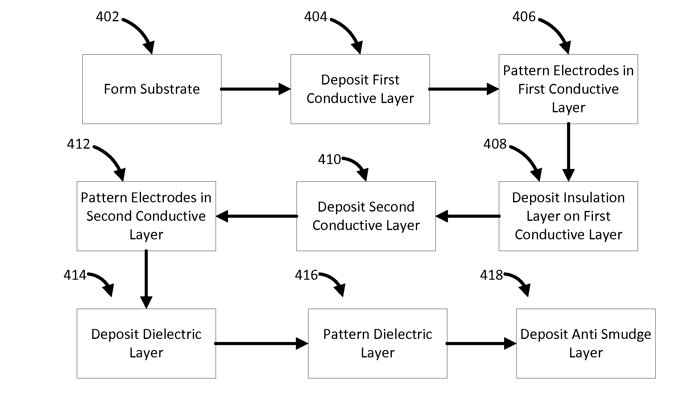
[0044]Within the teachings of this disclosure, a touch interface providing simultaneous touch sensing and haptic actuation is manufactured by depositing and patterning a series of layers on the front (touch) surface of an insulating substrate. The substrate may be either a rigid material, such as glass, or a flexible material, such as plastic. A first conductive layer, comprising a conductive material, may serve as a first axis of electrodes (for example, an x axis if there are two axes). An insulating layer, comprising an insulating material, may serve as an insulator and may be either patterned to form individual insulator patches at each desired x-y intersection (bridges) or applied as a full continuous sheet. A second conductive layer, comprising a conducting material, may serve as a second axis of electrodes (for example, a y axis if there are two axes). Additional alternating insulating and conducting layers may be provided for additional electrodes. After all electrode layers...


PUM


Abstract

A haptic interface device, said device comprising a substrate, a first conducting layer deposited on the substrate, with the first conducting layer being patterned to provide a first axis of individually-addressable conductive electrodes, a first insulating layer deposited on the first conducting layer, with the insulating layer having a uniform thickness, a second conducting layer deposited on the first insulating layer, with the second conducting layer being patterned to provide a second axis of individually-addressable conductive electrodes, and a dielectric layer deposited on the second conducting layer, with the dielectric layer having a uniform thickness and hardness and being scratch resistant.

Description

CROSS-REFERENCE TO RELATED APPLICATIONS[0001]This application is a non-provisional patent application that claims the benefit of and the priority from U.S. Provisional Patent Application No. 62 / 074,362, filed Nov. 3, 2014, titled MATERIALS AND STRUCTURES FOR HAPTIC DISPLAYS WITH SIMULTANEOUS SENSING AND ACTUATION.STATEMENT REGARDING FEDERALLY SPONSORED RESEARCH OR DEVELOPMENT[0002]This invention was made with government support under grant number IIP-1330966 awarded by the National Science Foundation. The government has certain rights in the invention.BACKGROUND OF THE INVENTION[0003]The present disclosure generally relates to touch interface devices and more particularly to constructions and methods of construction for touch surfaces of such devices that provide touch sensing input and haptic output.[0004]Touch interfaces can be found in laptop computers, gaming devices, automobile dashboards, kiosks, operating rooms, factories, automatic tellers, and a host of portable devices suc...

Claims


Application Information

Patent Timeline
Patent Type & Authority Applications(United States)
IPC IPC(8): G06F3/044G06F3/01B05D7/00G06F3/041
CPCG06F3/044G06F3/0412G06F2203/04103B05D7/58G06F3/016G06F3/0445
Inventor CHERIF, MONDHERCOLGATE, JAMES E.PESHKIN, MICHAEL A.OLLEY, MICHAEL F.D.TOPEL, GREGORY
Owner TANVAS INC
Why Eureka
Try Eureka