Semiconductor device

Active Publication Date: 2016-06-09
SK HYNIX INC
View PDF3 Cites 19 Cited by
  • Summary
  • Abstract
  • Description
  • Claims
  • Application Information

AI Technical Summary

Benefits of technology

[0016]In an embodiment, a semiconductor device may include a plurality of channels formed in a single package, and may be configured to share calibration information through exchanging signals and data among respective dies. The semiconductor device may include ZQ driving blocks respectively provided in the plurality of

Problems solved by technology

However, the SDR synchronous memory device has difficulty

Method used


Image

  • Semiconductor device
  • Semiconductor device
  • Semiconductor device

Examples


Embodiment Construction

[0024]Hereinafter, a semiconductor device will be described below with reference to the accompanying drawings through various examples of embodiments.

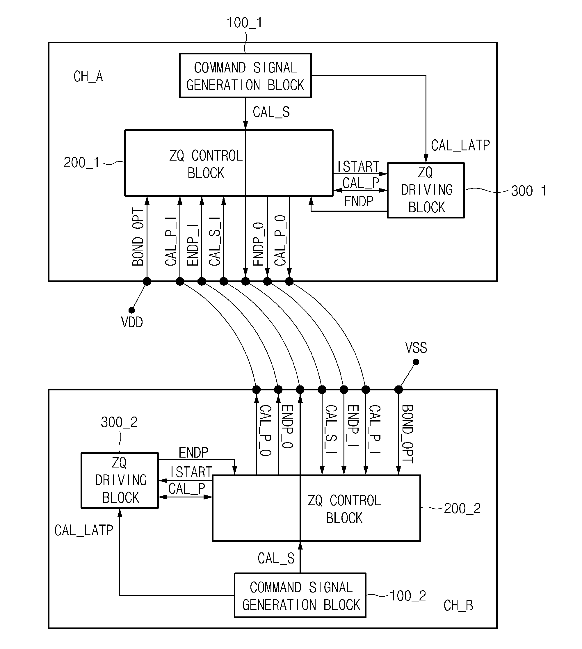
[0025]In the examples of configuring 2 channels by packaging 2 dies, considerations should be made for the ZQ pins.

[0026]Various embodiments may be directed to a technology for controlling the ZQ calibration timing of a multi-channel semiconductor device including two dies configured as a single chip.

[0027]According to various embodiments, it may be possible to independently control ZQ calibration in correspondence to PVT (process, voltage and temperature) in a multi-channel semiconductor device including two dies configured as a single chip.

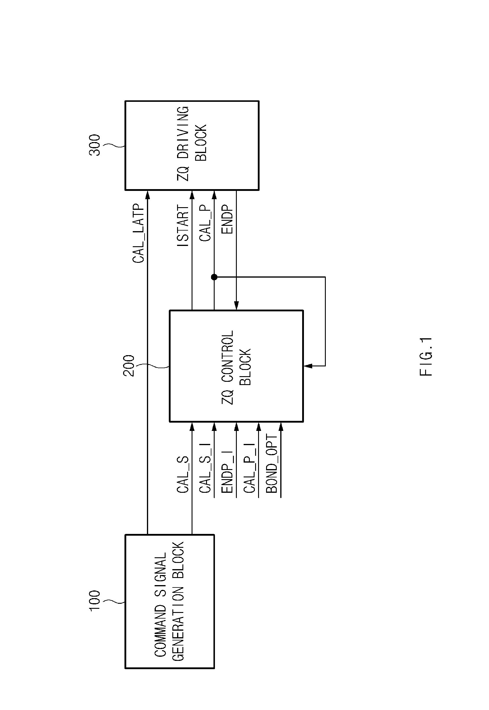
[0028]FIG. 1 is a configuration diagram illustrating a representation of an example of a semiconductor device in accordance with an embodiment.

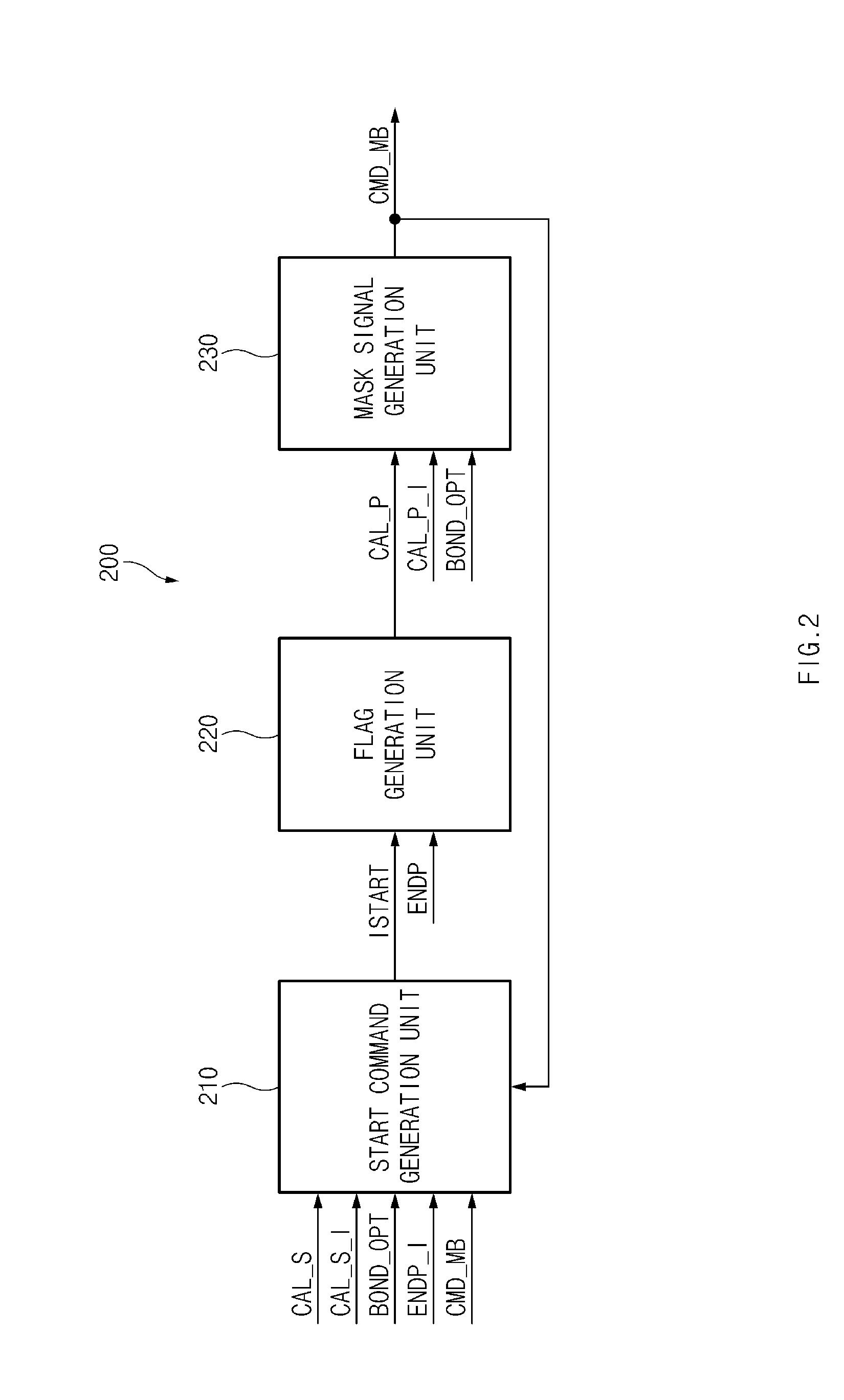
[0029]The semiconductor device in accordance with an embodiment may include a command signal generation block 100, a ZQ control block 200, and a ZQ driving ...


PUM


Abstract

A semiconductor device may include a first channel provided in a first die. The semiconductor device may include a second channel provided in a second die and disposed adjacent to the first channel, and configured to exchange signals and data with the first channel. The first channel and the second channel may receive and output calibration-related signals from and to each other through bonding, and may share calibration start signals. The calibration start signal may be respectively generated in the first channel and the second channel.

Description

CROSS-REFERENCES TO RELATED APPLICATION[0001]The present application claims priority under 35 U.S.C. §119(a) to Korean application number 10-2014-0174068, filed on Dec. 5, 2014, in the Korean Intellectual Property Office, which is incorporated herein by reference in its entirety.BACKGROUND[0002]1. Technical Field[0003]Various embodiments generally relate to a semiconductor device, and more particularly, to a technology for controlling ZQ calibration of a semiconductor device including two dies configured as a single chip.[0004]2. Related Art[0005]Developments are being made to increase the degree of integration and the operating speeds of semiconductor memory devices. Synchronous memory devices have been developed to increase the operating speeds of the semiconductor memory devices. These synchronous memory devices are capable of operating in synchronization with a clock signal received from outside a memory chip.[0006]For example, an SDR (single data rate) synchronous memory device...

Claims


Application Information

Patent Timeline
IPC IPC(8): H03K19/0175
CPCH03K19/017509G11C7/1057G11C7/1084G11C2207/2254G11C11/4093H03K19/017545G11C7/1009G11C7/1093G11C7/222G11C7/225G11C11/401G11C11/4076G11C2211/4061
Inventor CHUNG, WON KYUNGKIM, SAENG HWAN
Owner SK HYNIX INC
Why Eureka
Try Eureka