Method of selective gas phase film deposition on a substrate

Active Publication Date: 2016-06-16
TOKYO ELECTRON LTD
View PDF4 Cites 250 Cited by
  • Summary
  • Abstract
  • Description
  • Claims
  • Application Information

AI Technical Summary

Problems solved by technology

As device size is getting smaller at the 14 nm technology node, the complexity in manufacturing is increasing.
As smaller transistors are manufactured, the critical dimension (CD) or resolution of

Method used


Image

  • Method of selective gas phase film deposition on a substrate
  • Method of selective gas phase film deposition on a substrate
  • Method of selective gas phase film deposition on a substrate

Examples


Example

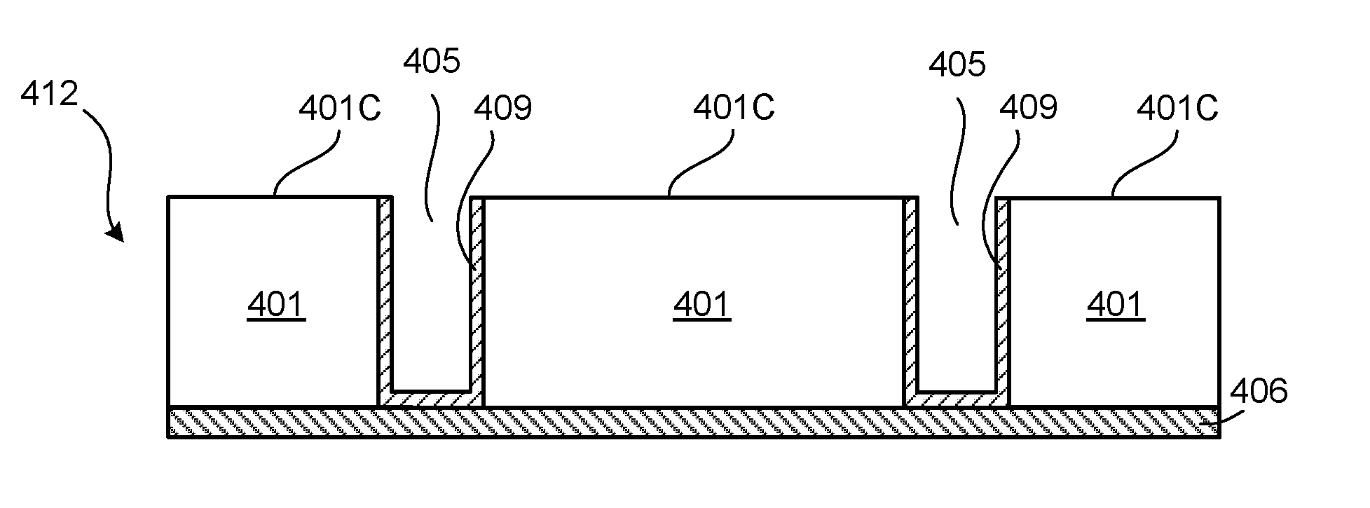
[0019]Some embodiments of the invention provide a non-polymer based approach to selectively depositing a film (e.g., insulator or metal) on a desired surface of a substrate while inhibiting the film deposition on the rest of the substrate. This reduces or eliminates the need for additional patterning steps that normally include lithography and etching steps. The selective film deposition can be achieved after surface modification using hydrogen gas that is plasma excited and exposed to the substrate. According to one embodiment, the hydrogen gas may be excited using a microwave plasma source. According to other examples, other plasma sources may be used, including an inductively couple plasma (ICP) source and a capacitively coupled plasma (CCP) source.

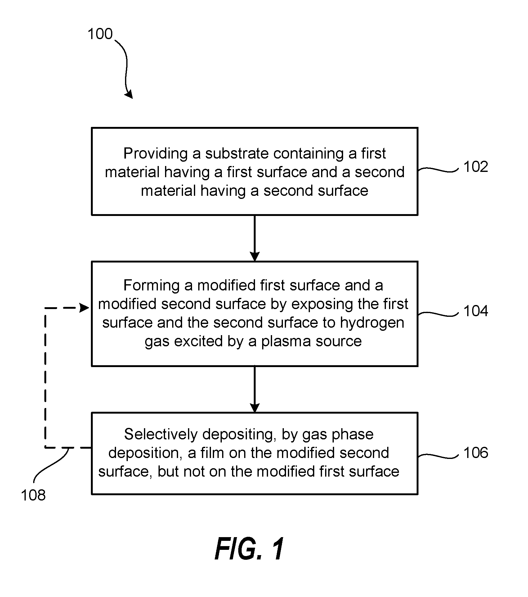
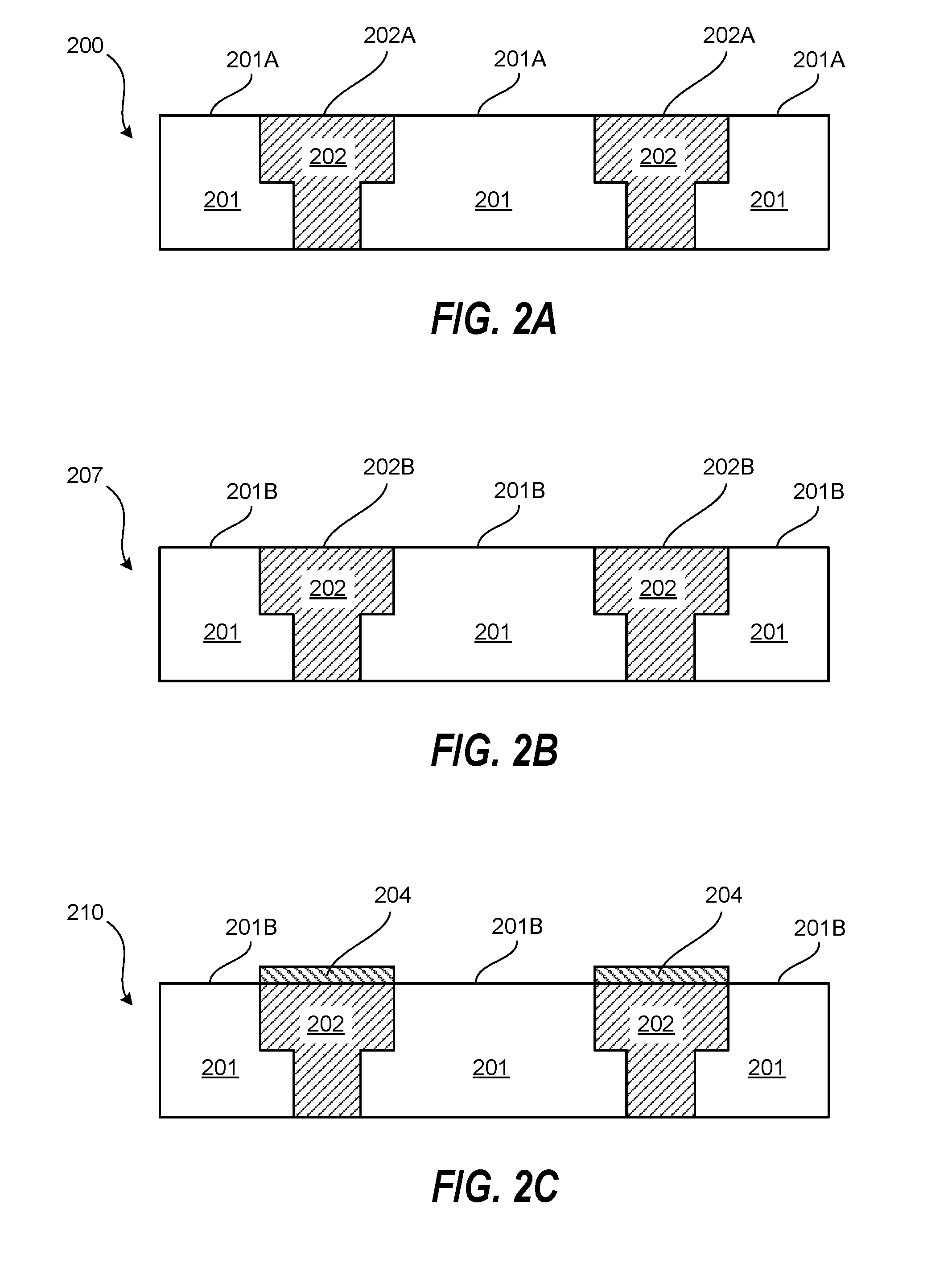
[0020]Embodiments of the invention are described below in reference to the Figures. According to one embodiment, a method is provided for selective film deposition on a substrate. The method includes providing a substrate containing a ...


PUM

PropertyMeasurementUnit
Dielectric polarization enthalpyaaaaaaaaaa
Semiconductor propertiesaaaaaaaaaa

Abstract

According to one embodiment of the invention, a method is provided for selective surface deposition. In one example, the method includes providing a substrate containing a first material having a first surface and a second material having a second surface, forming a modified first surface and a modified second surface by exposing the first surface and the second surface to hydrogen gas excited by a plasma source, and selectively depositing a film on the modified second surface but not on the modified first surface.

Description

CROSS-REFERENCE TO RELATED APPLICATIONS[0001]This application is related to and claims priority to U.S. Provisional Patent Application Ser. No. 62 / 092,157 filed on Dec. 15, 2014, the entire contents of which are herein incorporated by reference.FIELD OF THE INVENTION[0002]The present invention generally relates to a method of selective deposition of a film on different material surfaces using gas phase deposition.BACKGROUND OF THE INVENTION[0003]As device size is getting smaller at the 14 nm technology node, the complexity in manufacturing is increasing. The cost to produce the semiconductor devices is also increasing and cost effective solutions and innovations are needed. As smaller transistors are manufactured, the critical dimension (CD) or resolution of patterned features is becoming more challenging to produce. Self-aligned patterning may replace overlay-driven patterning so that cost-effective scaling can continue even after EUV introduction. Patterning options that enable re...

Claims


Application Information

Patent Timeline
IPC IPC(8): H01L21/02
CPCH01L21/02172H01L21/0228H01L21/02315C23C16/045C23C16/403C23C16/405C23C16/4554C23C16/511H01L21/02178H01L21/02252H01L21/02296H01L21/02299H01L21/3003H01L21/76814H01L21/76826H01L21/76831H01L21/76834H01L21/76883
Inventor TAPILY, KANDABARA N.
Owner TOKYO ELECTRON LTD
Why Eureka
Try Eureka