

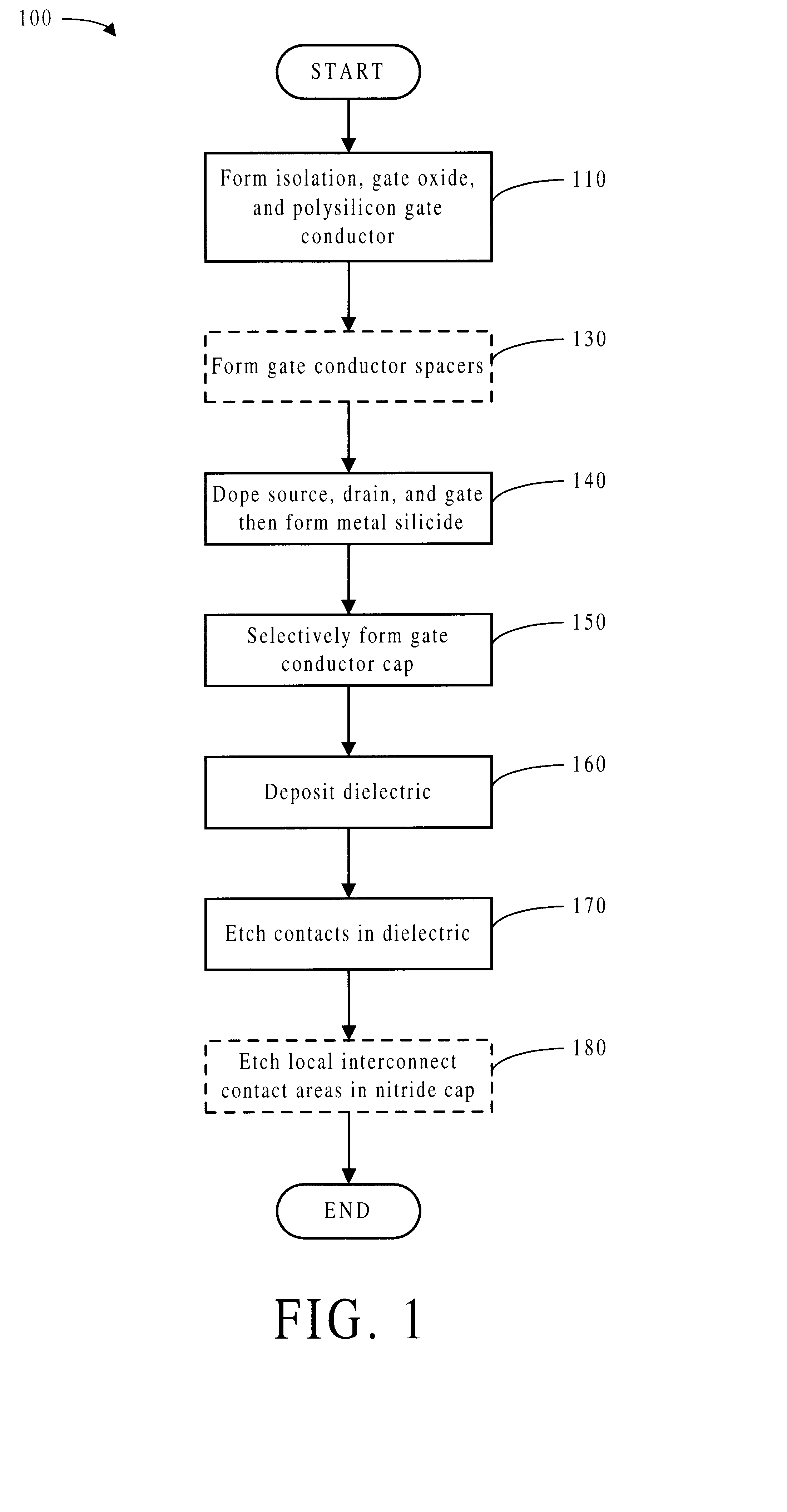
Method for forming borderless gate structures and apparatus formed thereby
a gate structure and apparatus technology, applied in the field of methods, can solve the problems of consuming a great deal of chip area, further increasing circuit density, and the method of protecting gate conductors with etch-stop dielectric 560 possesses several limitations, so as to reduce the effect of reducing the power and reducing the resistance of the sh
- Summary
- Abstract
- Description
- Claims
- Application Information
AI Technical Summary
Benefits of technology
Problems solved by technology
Method used
Image

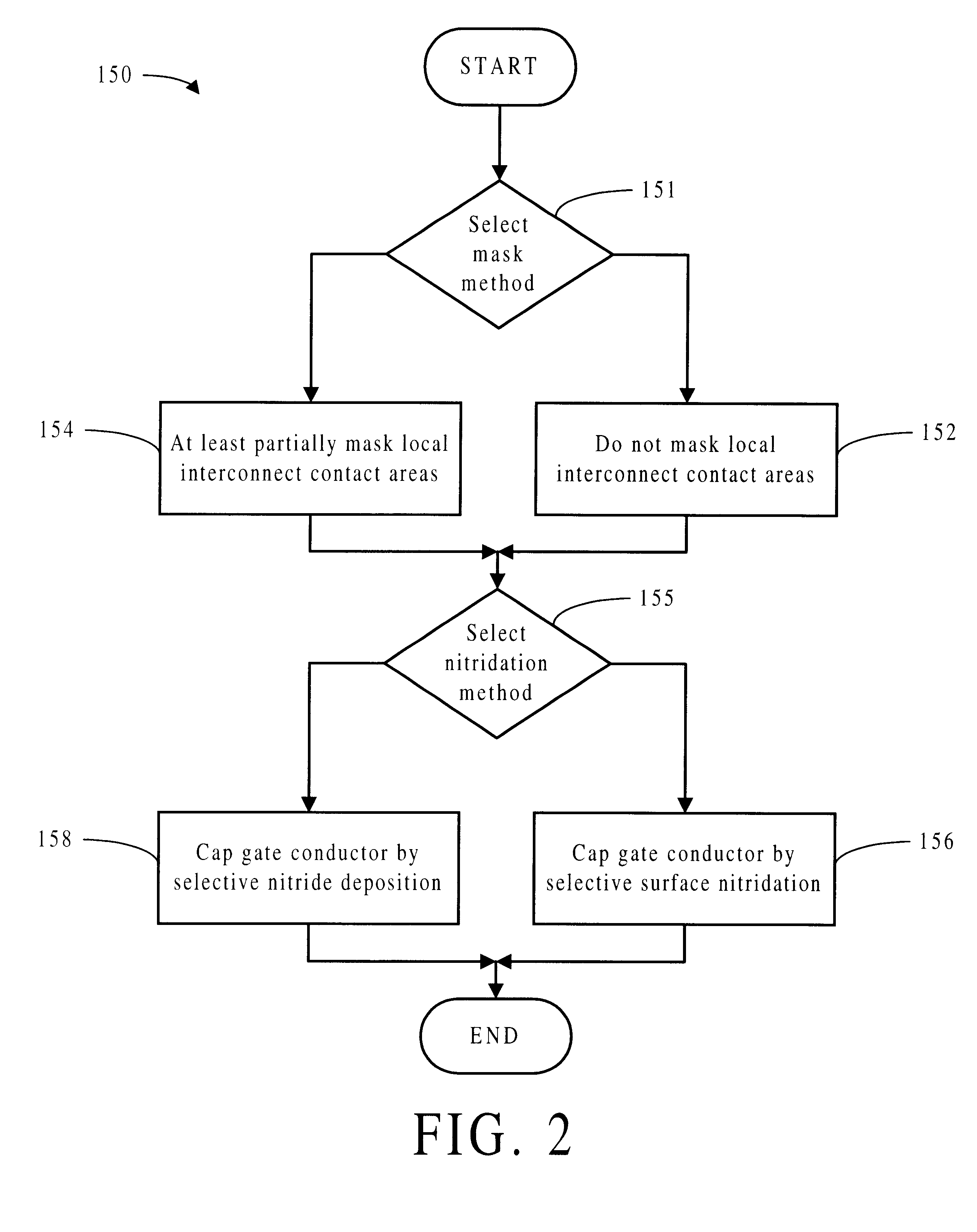
Examples
example 2
Selective Nitride Deposition From Silane and Ammonia. A silicon wafer substrate is prepared as above, with isolation, diffusion and gate structures. In this embodiment, it is not necessary to melt the surface of the polysilicon in order to deposit the nitride. As such, the energy fluence per pulse at the wafer surface can range from about 100-500 mJ / cm.sup.2, with preferred expose values of about 300 mJ / cm.sup.2. The number of expose pulses can range from 10 to 1000, depending on the desired thickness of deposited nitride; preferred values are from 50-300 pulses. The substrate temperature can range between 500 and 1200.degree. C., with values of about 850.degree. C. being preferable as indicated in U.S. Pat. No. 4,592,933 to Meyerson et al, that is incorporated herein by reference.
During the expose, the ammonia and silane gases are placed in the immediate environment of the wafer. This is accomplished by utilizing the evacuation and chemical injection system of the Verdant Technolog...
example 3
Selective Surface Nitridation of the Polysilicon Gate with Ammonia. A silicon wafer substrate is prepared as above, with isolation, diffusion and gate structures. In place of depositing a silicon nitride layer on the gate conductor by exposing the irradiated wafer to silane and ammonia, the irradiated wafer is exposed only to ammonia vapor. When a melted silicon film (melted by laser irradiation at 308 nm) is exposed to ammonia, a silicon nitride film can be formed in the surface of the silicon. Films as thick as 500 nm may be grown by this method. In a polysilicon gate according to the present invention, 50-100 nm of nitride are desirable so the sample is irradiated with an energy fluence of 200-700 mJ / cm.sup.2 per pulse, or more preferably 400-500 mJ / cm.sup.2, in the presence of 10-1500 torr of ammonia, or more preferably about 1200 torr ammonia, at 100 ccm / min for a duration of 100-2000 pulses, or more preferably about 300 pulses. The polysilicon is selectively heated by the 308-...
PUM
 Abstract
Description
Claims
Application Information