Flash Memory Device Configurable To Provide Read Only Memory Functionality

Active Publication Date: 2016-08-18
SILICON STORAGE TECHNOLOGY
View PDF3 Cites 1 Cited by
  • Summary
  • Abstract
  • Description
  • Claims
  • Application Information

AI Technical Summary

Problems solved by technology

However, the prior art does not contain a flash memory devices that can operate as a read only memory device, or which can

Method used


Image

  • Flash Memory Device Configurable To Provide Read Only Memory Functionality
  • Flash Memory Device Configurable To Provide Read Only Memory Functionality
  • Flash Memory Device Configurable To Provide Read Only Memory Functionality

Examples


Embodiment Construction

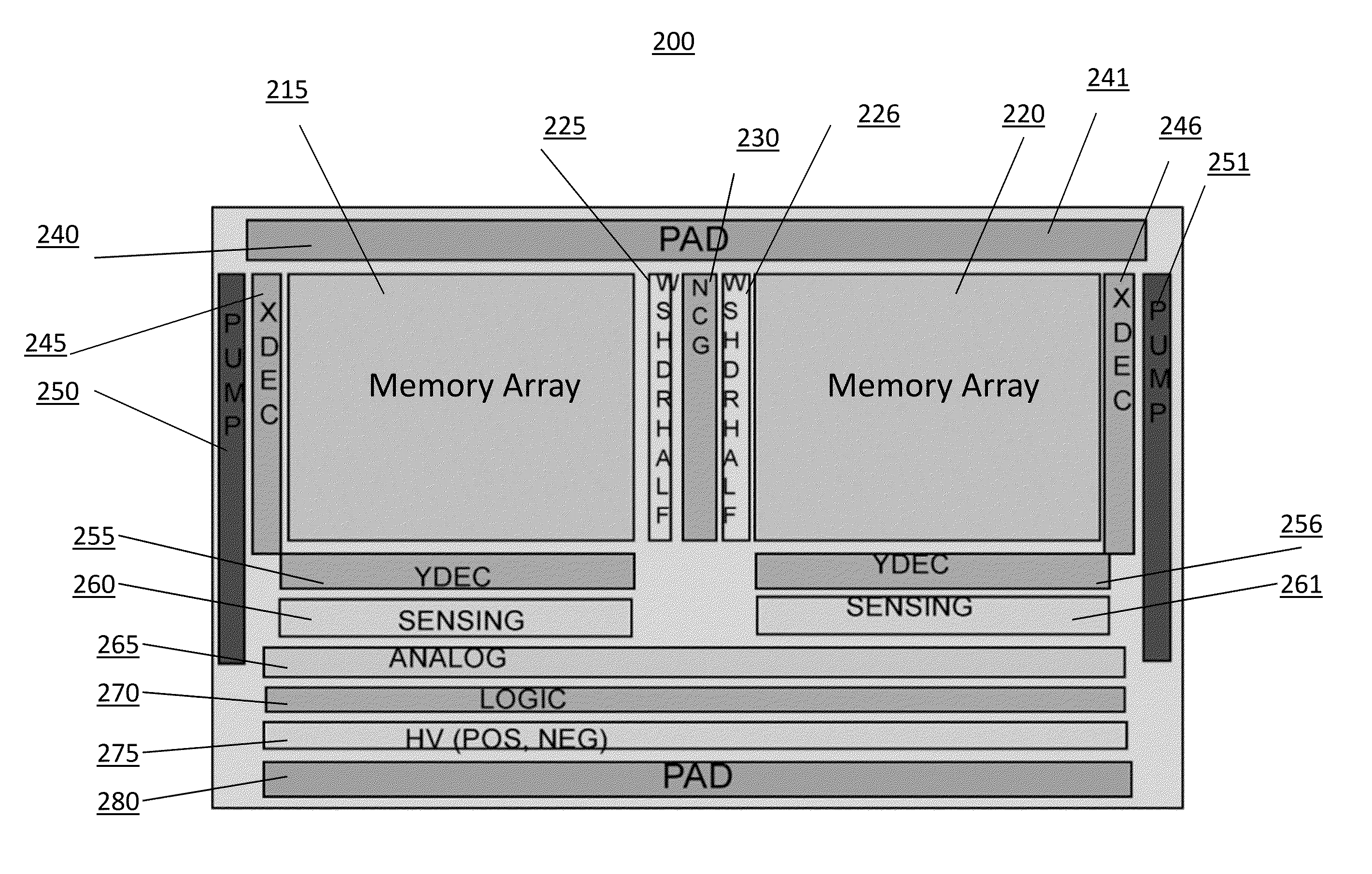
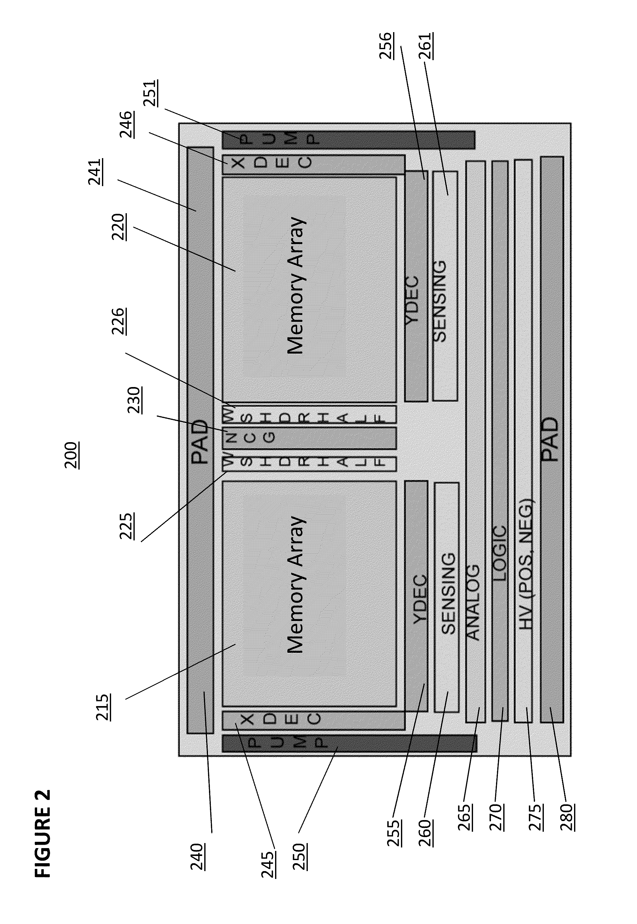
[0018]FIG. 2 depicts an embodiment of an architecture for a flash memory system comprising die 200. Die 200 comprises: memory array 215 and memory array 220 for storing data, memory arrays 215 and 220 comprising rows and columns of memory cells of the type described previously as memory cell 10 in FIG. 1, pad 240 and pad 280 for enabling electrical communication between the other components of die 200 and, typically, wire bonds (not shown) that in turn connect to pins (not shown) or package bumps that are used to access the integrated circuit from outside of the packaged chip or macro interface pins (not shown) for interconnecting to other macros on a SOC (system on chip); high voltage circuit 275 used to provide positive and negative voltage supplies for the system; control logic 270 for providing various control functions, such as redundancy and built-in self-testing; analog circuit 265; sensing circuits 260 and 261 used to read data from memory array 215 and memory array 220, res...


PUM


Abstract

The disclosed embodiments comprise a flash memory device that can be configured to operate as a read only memory device. In some embodiments, the flash memory device can be configured into a flash memory portion and a read only memory portion.

Description

TECHNICAL FIELD[0001]The disclosed embodiments comprise a flash memory device that can be configured to operate as a read only memory device. In some embodiments, the flash memory device can be configured into a flash memory portion with variable flash array size and a read only memory (ROM) portion with variable ROM array size.BACKGROUND OF THE INVENTION[0002]Non-volatile memory cells are well known in the art. One prior art non-volatile split gate memory cell 10 is shown in FIG. 1. The memory cell 10 comprises a semiconductor substrate 12 of a first conductivity type, such as P type. The substrate 12 has a surface on which there is formed a first region 14 (also known as the source line SL) of a second conductivity type, such as N type. A second region 16 (also known as the drain line) also of N type is formed on the surface of the substrate 12. Between the first region 14 and the second region 16 is a channel region 18. A bit line BL 20 is connected to the second region 16. A wor...

Claims


Application Information

Patent Timeline
IPC IPC(8): G11C16/08G11C17/08G11C16/22G11C16/14G11C16/26
CPCG11C16/08G11C16/14G11C2216/26G11C16/22G11C17/08G11C16/26
Inventor TRAN, HIEU VANLY, ANHVU, THUANNGUYEN, HUNG QUOC
Owner SILICON STORAGE TECHNOLOGY
Why Eureka
Try Eureka