Electronic device

a technology of electronic devices and display regions, applied in the field of electronic devices, can solve the problems of reducing portability, difficult to improve display and portability, and large display regions, and achieve the effect of improving portability and large display regions of electronic devices

Active Publication Date: 2017-05-18
SEMICON ENERGY LAB CO LTD
View PDF5 Cites 75 Cited by
  • Summary
  • Abstract
  • Description
  • Claims
  • Application Information

AI Technical Summary

Benefits of technology

[0010]An object of one embodiment of the present invention is to provide an electronic device with a large display region. Another object is to improve the portability of an electronic device. Another object is to provide an electronic device in which the size of a display region can be changed. Another object is to provide an electronic device in which the size of a display region can be selected depending on the intended use. Another object is to provide a novel electronic device.
[0022]According to one embodiment of the present invention, an electronic device with a large display region is provided. In addition, the portability of an electronic device is improved. In addition, an electronic device in which the size of a display region can be changed is provided. In addition, an electronic device in which the size of a display region can be selected depending on the intended use is provided. In addition, a novel electronic device is provided.

Problems solved by technology

However, in portable electronic devices, large display regions might entail a reduction in portability.
For this reason, the browsability of display and portability are difficult to improve at the same time.

Method used


Image

  • Electronic device
  • Electronic device
  • Electronic device

Examples


embodiment 1

[0053]In this embodiment, structural examples of an electronic device of one embodiment of the present invention will be described.

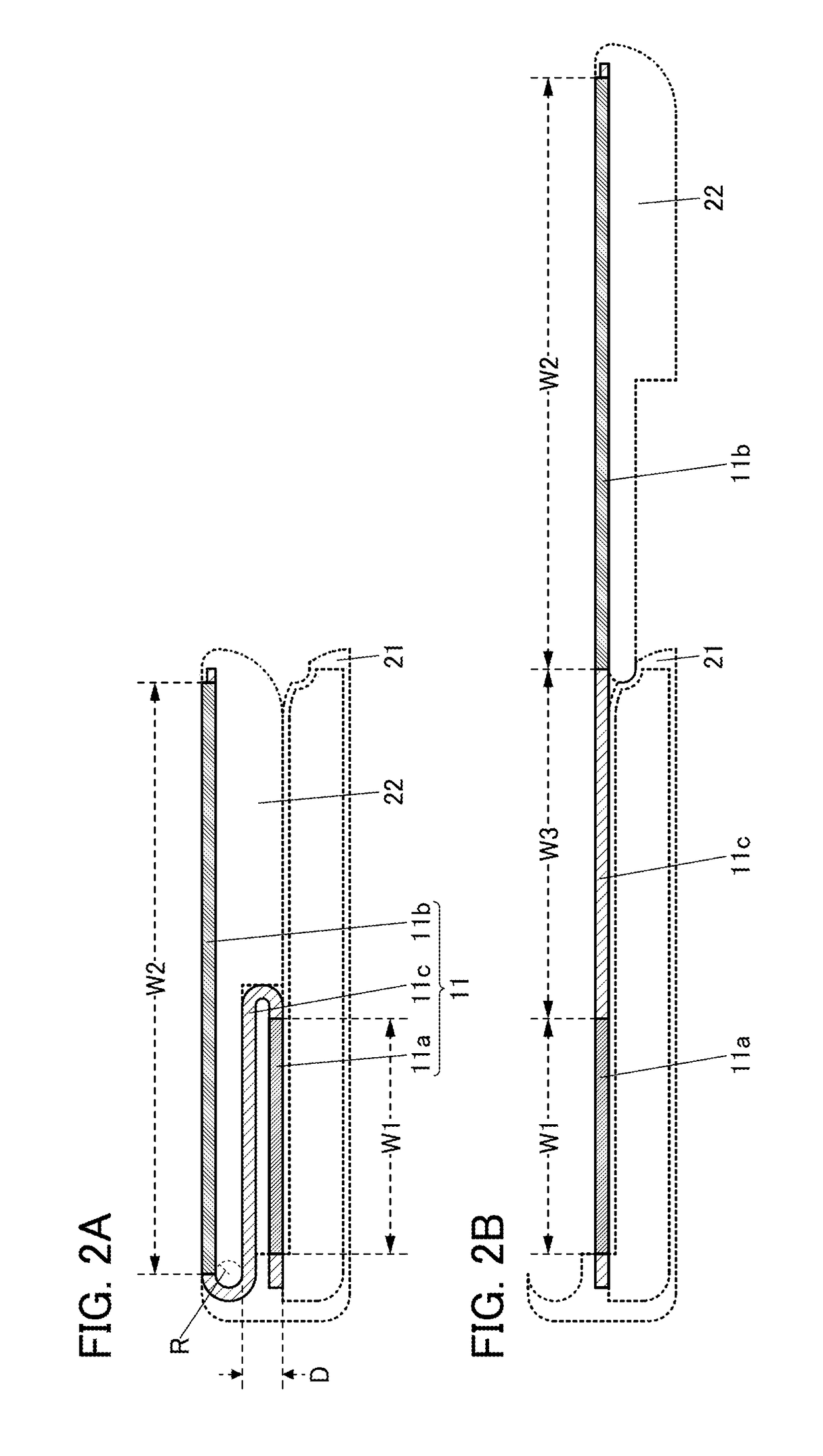
[0054]An electronic device of one embodiment of the present invention includes a display panel which is partly flexible and bendable. The electronic device can take two forms of a form in which the display panel is opened and a form in which the display panel is folded in three.

[0055]The electronic device has a structure in which two portions between which a bent portion of the display panel is positioned are each fixed to a housing. In the form in which the display panel is folded in three, the display panel includes a portion where a display surface is convexly curved and a portion where the display surface is concavely curved. In addition, when the electronic device includes a mechanism for sliding the two housings parallel to each other, the display panel can be changed in shape so that the two curved portions move in directions parallel and opposite...

modification example

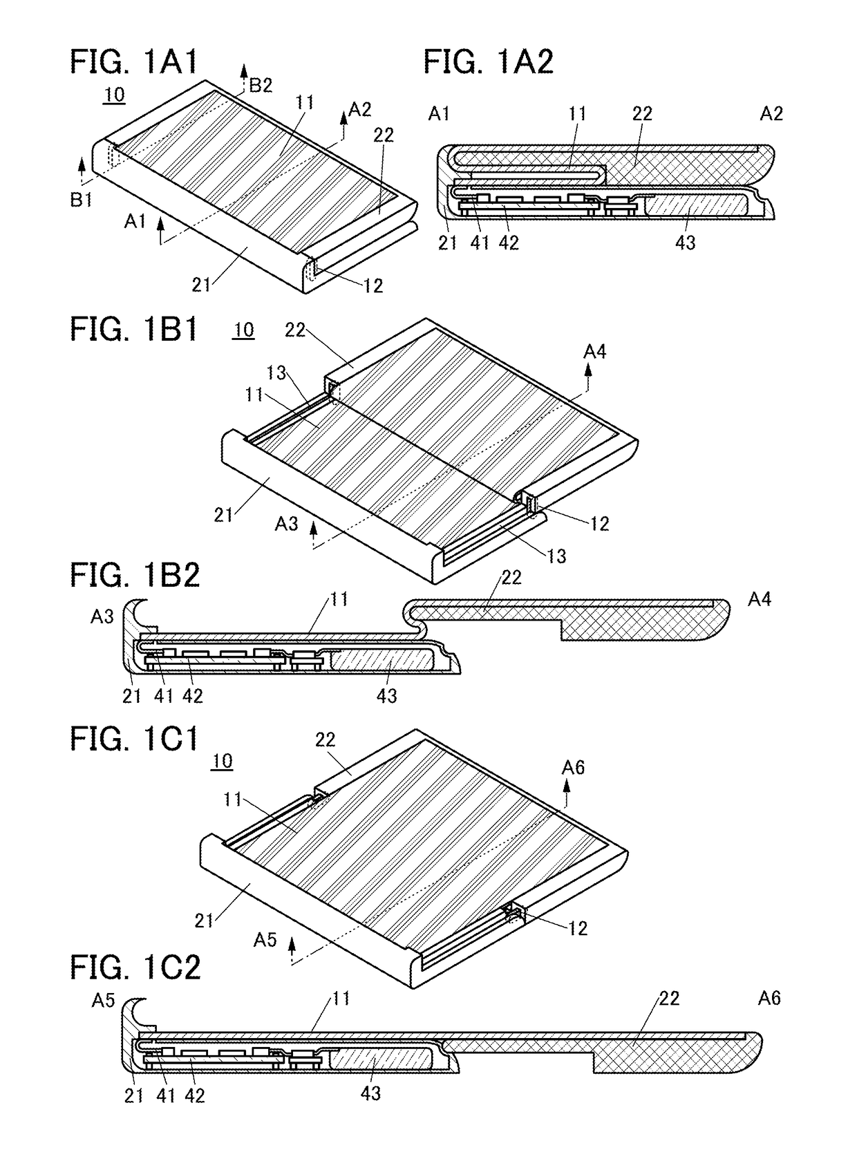
[0115]Structural examples of the electronic device 10 whose structure is partly different from the above structures will be described below.

[0116]FIG. 9A is a schematic cross-sectional view of the electronic device 10 in the state where the display panel 11 is folded. In FIG. 9A, a portion positioned between two curved portions of the flexible portion 11c of the display panel 11 extends not in a direction parallel to the portion 11a and the portion 11b but in an oblique direction. Specifically, the portion where the display surface is convexly curved and the portion where the display surface is concavely curved of the portion 11c are each curved at an angle less than 180°. With such a structure, when the housing 21 and the housing 22 are slid so as to be closed, the direction of force which is applied when the portion 11c of the display panel 11 is pulled can be an obliquely above direction. Accordingly, the portion 11c can be changed in shape more easily than the case of FIG. 2A.

[0...

application example

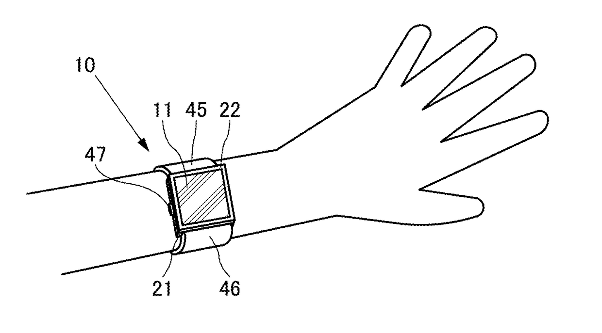
[0196]One embodiment of the present invention can be used as a wearable electronic device (wearable device).

[0197]FIG. 14 illustrates an example of a watch-type wearable device including the electronic device 10. The wearable device illustrated in FIG. 14 includes the electronic device 10, a band 45, a band 46, and the like. The band 45 includes a buckle and the band 46 includes a plurality of holes engaging with the buckle. The wearable device can be worn on an arm or the like with the two bands. Note that the structure of the band is not limited thereto, and a variety of bands can be used.

[0198]When the display panel 11 has a function as a touch panel, the electronic device 10 can be operated by touch on the display region.

[0199]Furthermore, FIG. 14 illustrates an example in which a housing button 47 is provided on the side surface of the housing 21 of the electronic device 10. As the input operation using the housing button 47, operations such as touching, pushing, turning, pulli...


PUM


Abstract

An electronic device has a structure in which two portions between which a bent portion of a display panel is positioned are each fixed to a housing. The electronic device takes two forms of a form in which the display panel is opened and a form in which the display panel is folded in three. The electronic device includes a mechanism for sliding two housings parallel to each other. The display panel is changed in shape so that a portion where a display surface of the display panel is convexly curved and a portion where the display surface of the display panel is concavely curved in the folded state move in directions parallel and opposite to each other. At this time, the two portions of the display panel which are supported by the housings are slid while their display surfaces maintain a state parallel to each other.

Description

BACKGROUND OF THE INVENTION[0001]1. Field of the Invention[0002]One embodiment of the present invention relates to an electronic device including a display device.[0003]Note that one embodiment of the present invention is not limited to the above technical field. Examples of the technical field of one embodiment of the present invention disclosed in this specification and the like include a semiconductor device, a display device, a light-emitting device, a power storage device, a memory device, an electronic device, a lighting device, an input device, an input / output device, a method for driving any of them, and a method for manufacturing any of them.[0004]2. Description of the Related Art[0005]Electronic devices including display devices have recently been diversified. Examples of the electronic devices include cellular phones, smartphones, tablet terminals, and wearable terminals.[0006]Examples of the display device include, typically, a light-emitting device including a light-emi...

Claims


Application Information

Patent Timeline
Patent Type & Authority Applications(United States)
IPC IPC(8): G06F1/16G04G9/04H04M1/02
CPCG06F1/1641G06F1/163G06F1/1652G06F1/1681G06F1/1626H04M1/0268H01L2251/5315G06F1/1643G04G9/04H04M2201/38H01L27/323H01L27/3244H01L51/52H04M1/0237G04G17/045G06F1/1624H04M1/0239H04M1/0247H04M2250/16H04M2250/22C09K2323/00H10K59/10H10K59/40H10K50/80H10K59/12H10K2102/3026
Inventor YOSHIZUMI, KENSUKE
Owner SEMICON ENERGY LAB CO LTD
Why Eureka
Try Eureka