
Controlled synthesis and transfer of large area heterostructures made of bilayer and multilayer transition metal dichalocogenides

a technology of transition metal dichalocogenide and heterostructure, which is applied in the field of bilayer and multilayer transition metal dichalocogenide systems, can solve problems such as not being reported theoretically or experimentally

Active Publication Date: 2018-02-08
PENN STATE RES FOUND
View PDF2 Cites 5 Cited by
  • Summary
  • Abstract
  • Description
  • Claims
  • Application Information

AI Technical Summary

Problems solved by technology

So far, it has been not been reported theoretically or experimentally that it is possible to generate a direct band gap in bilayer and multilayer systems if the layers and the stackings are different in chemical composition.

Method used


Image

  • Controlled synthesis and transfer of large area heterostructures made of bilayer and multilayer transition metal dichalocogenides
  • Controlled synthesis and transfer of large area heterostructures made of bilayer and multilayer transition metal dichalocogenides
  • Controlled synthesis and transfer of large area heterostructures made of bilayer and multilayer transition metal dichalocogenides

Examples


Embodiment Construction

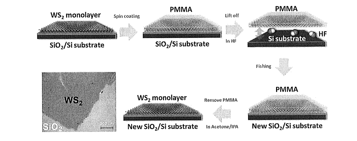
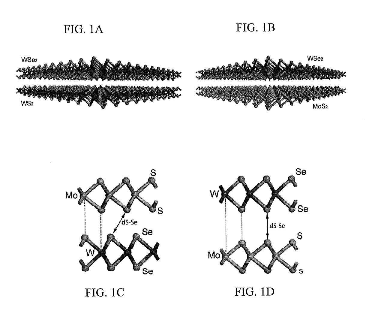
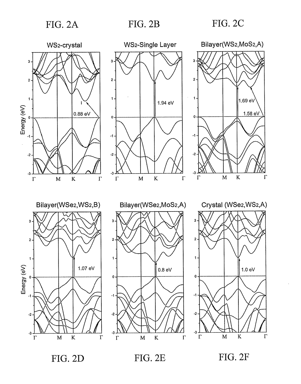
[0029]We have found that direct band gaps may be obtained by sandwiching different metal disulfides and diselenides.

[0030]We have demonstrated, for the first time, that it is possible to obtain novel direct band gap bilayers of STMD if different monolayers are overlapped. Moreover, in some cases it is possible to have direct band gap crystals with an infinite number of layers if the stacking belongs to A type. The direct band gap bilayers exhibit a physical separation of electron and holes probably due to a sort of local Giant Stark Effect caused by charge differences established between the heterogeneous layers. In these systems, the top of the valence band is dominated by the selenide layer and the bottom of the conduction band is controlled by the states of the sulfide layer. Homogeneous bilayers of TMD do not possess this net charge separation and hence do not exhibit direct band gaps. In addition, this is a different behavior from that found for monolayers of STMD, in which ele...


PUM

PropertyMeasurementUnit
band gapaaaaaaaaaa
band gapaaaaaaaaaa
excitation wavelengthaaaaaaaaaa

Abstract

Embodiments are presented herein that provide a TMD system wherein the first layered material is made of heterobilayers or multilayers with semiconducting direct band gaps. The first layered material may be made of multiple layers of different TMD with different stackings, exhibiting smaller direct and indirect band gaps smaller than monolayer systems of TMD.

Description

CROSS-REFERENCE TO RELATED APPLICATIONS[0001]This application claims benefit of U.S. Provisional Patent Application No. 61 / 805,461, filed on Mar. 26, 2013. That application is incorporated by reference herein.GOVERNMENT INTEREST[0002]This work is supported by the U.S. Army Research Office MURI grant W911NF-11-1-0362. The government may have rights in this invention.BACKGROUND OF THE INVENTIONField of the Invention[0003]Embodiments of the invention relate to bilayer and multilayer transition metal dichalcogenides systems and methods of making same.Description of the Related Art[0004]Bulk phases of trigonal prismatic transition metal dichalcogenides (TMD) can be semiconducting, metallic, or superconducting, depending on the atomic composition. Recently, it has been found that a monolayer of semiconducting MoS2, obtained by exfoliation, exhibits a direct band gap instead of having an indirect band gap as in the bulk. The same behavior has also been found for monolayers of MX2 where M i...

Claims


Application Information

Patent Timeline
Patent Type & Authority Applications(United States)
IPC IPC(8): H01L29/45H01L29/417H01L21/285
CPCH01L29/417H01L21/28556H01L29/45H01L29/24H01L21/02485H01L21/02499H01L21/02507H01L21/02568H01L21/768
Inventor TERRONES, HUMBERTOTERRONES, MAURICIOELIAS, ANA LAURAPEREA-LOPEZ, NESTOR
Owner PENN STATE RES FOUND
Learn More