

Multi-Layer Single Crystal 3D Stackable Memory
a stackable memory and multi-layer technology, applied in the direction of semiconductor devices, basic electric elements, electrical appliances, etc., can solve the problems of unacceptably high off current of diodes having both the anode and cathode regions of polycrystalline silicon, complex process for making such devices, and adversely affecting transistor performan
- Summary
- Abstract
- Description
- Claims
- Application Information
AI Technical Summary
Benefits of technology
Problems solved by technology
Method used
Image

Examples
Embodiment Construction
[0027]A detailed description of embodiments of the present technology is provided with reference to the Figures.
[0028]FIGS. 1-9 illustrate stages in a process flow for forming layers of single crystal semiconductor material separated by insulating material layers.
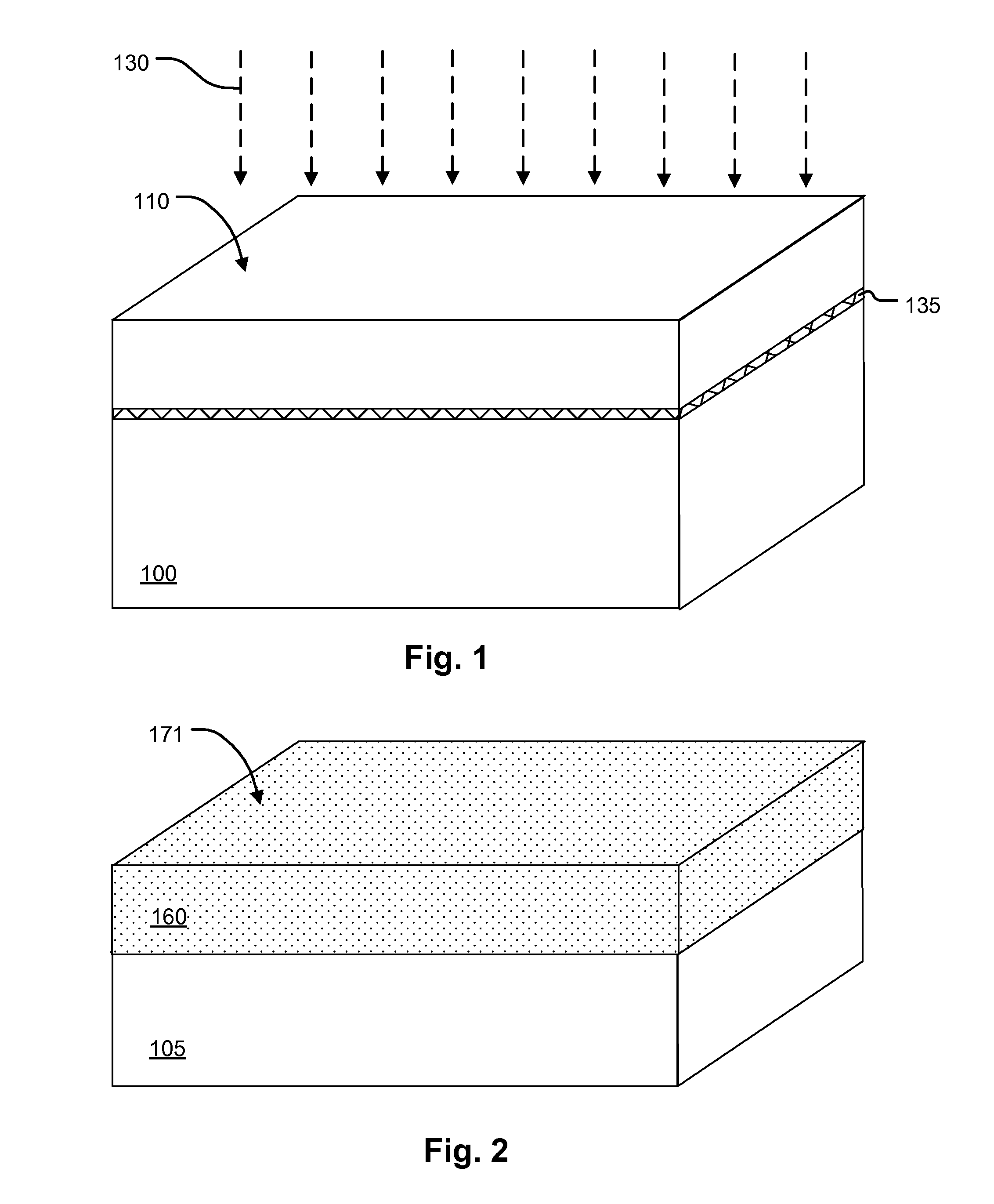
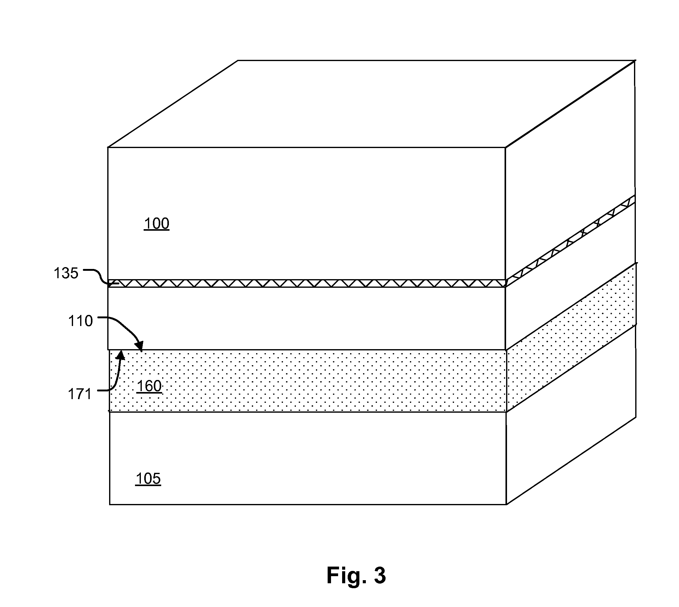
[0029]FIG. 1 shows the result of the formation of a single crystal semiconductor body 100 of silicon or other semiconductor material. The single crystal semiconductor body 100 is implanted with ions 130 of Hydrogen or a rare gas element, to form a defect layer 135 a predetermined depth from the top surface 110 of the first single crystal semiconductor body 100. In the illustrated embodiment, surface Hydrogen ion implantation is performed at a dosage range from 3e16 to 1e17 cm−2 at a temperature range from 225 to 300 degrees Celsius. In some embodiments, the implantation of the ions 130 can be performed in connection with the processes described for example in U.S. Pat. Nos. 5,374,564 and 5,993,667, which are incorporated by...
PUM
 Abstract
Description
Claims
Application Information