

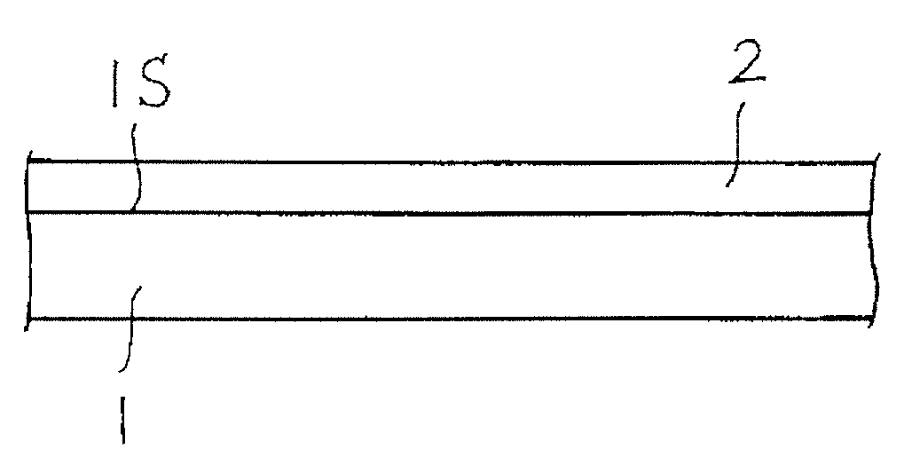
Nitride semiconductor wafer
a technology of nitride and semiconductor wafers, applied in the direction of silicon compounds, silicates, polycrystalline material growth, etc., can solve the problems of insufficient optical, electrical and mechanical properties, variation, and inability to solve simple problems, and achieve excellent properties and high quality
- Summary
- Abstract
- Description
- Claims
- Application Information
AI Technical Summary
Benefits of technology
Problems solved by technology
Method used
Image

Examples
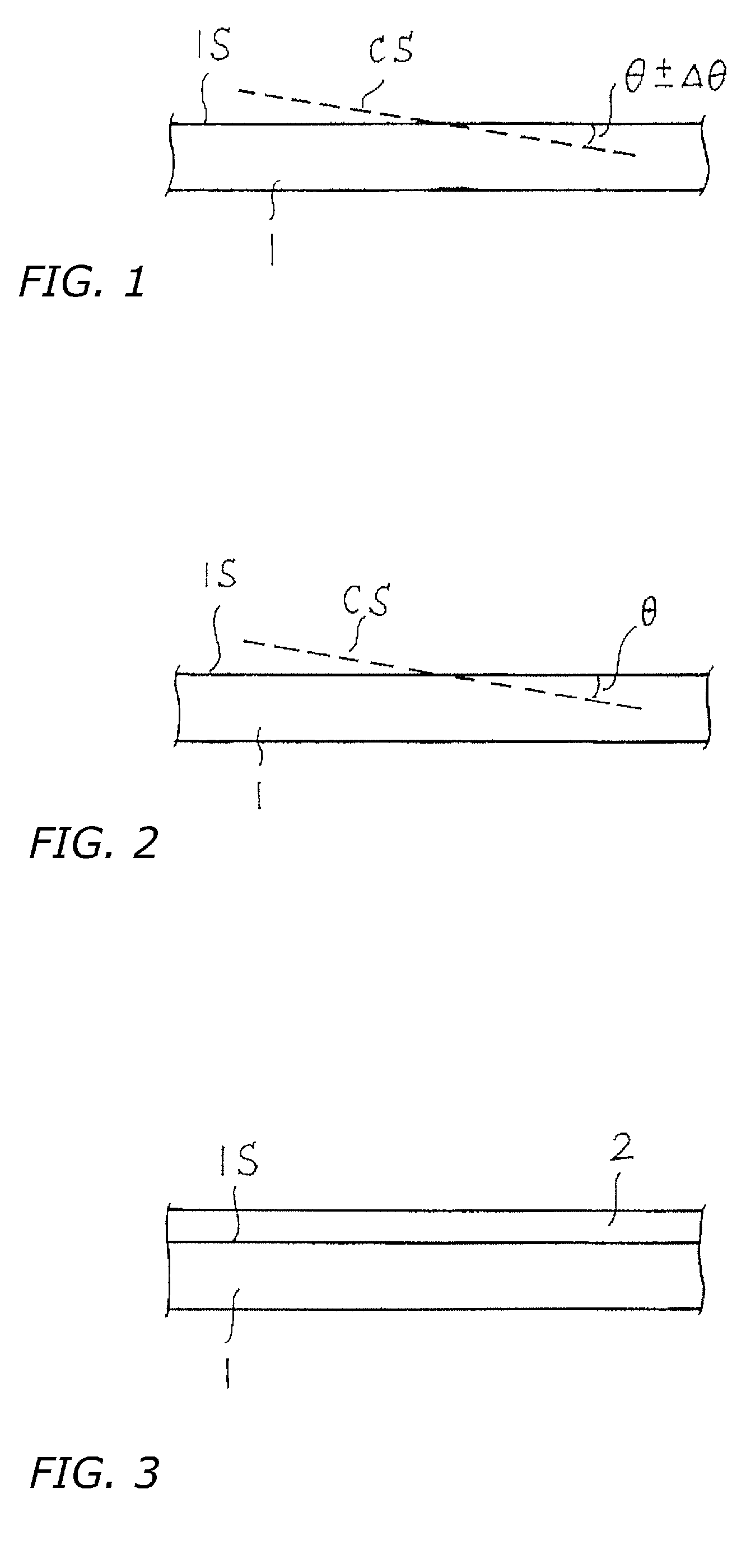
first embodiment
Δθ Less Than 1°
[0024]A nitride semiconductor substrate implementation in which the variation Δθ in off-axis angle θ is greater than 0° and less than 1°, makes it possible to obtain a substrate having uniform optical and electrical properties equal to those of the situation in which Δθ=0°, in which case there is absolutely no variation in the off-axis angle θ. In this implementation, the variation Δθ in the off-axis angle θ preferably is less than 0.5°. In the case of a nitride semiconductor substrate in which the variation Δθ in the off-axis angle θ is more than 0.05°, the direction of splitting due to cleavage of the nitride semiconductor substrate is dispersed, so mechanical properties with good resistance to cracking and breakage when processing and cutting the substrate are obtained. In this case, not less than 0.1° is preferable.
[0025]The variation Δθ in the off-axis angle θ can, for example, be obtained by measuring the off-axis angle θ in 5-mm intervals using XRD (X-ray diffr...
second embodiment
Δθ Not Less Than 1°
[0027]By performing epitaxial growth on the principal surface of a nitride semiconductor substrate in which the variation Δθ in the off-axis angle θ is not less than 1°, it is possible to efficiently identify the optimum off-axis angle of the nitride semiconductor substrate under exactly the same conditions as the conditions of actual production with a furnace in which an actual device structure is manufactured. That is, a nitride semiconductor substrate in which the variation Δθ in the off-axis angle θ is not less than 1° can be used as a substrate for finding the optimum off-axis angle θ.
[0028]Described more specifically, a satisfactory epitaxial growth layer is not obtained using the same substrate off-axis angle θ in all production devices; the optimum off-axis angle θ for the nitride semiconductor in a particular device changes depending on various factors, such as temperature, gas density, and gas flow rate. Given this understanding, by using, for example, a...
PUM
| Property | Measurement | Unit |
|---|---|---|
| off-axis angle | aaaaa | aaaaa |
| angle | aaaaa | aaaaa |
| misorientation angle | aaaaa | aaaaa |
Abstract
Description
Claims
Application Information