Method of forming a barrier film and method of forming wiring structure and electrodes of semiconductor device having a barrier film

a technology of a barrier film and a wiring structure, which is applied in the direction of semiconductor devices, semiconductor/solid-state device details, electrical equipment, etc., can solve the problems of gate electrode electrical resistance increase, inability to employ tin layer as a preferred barrier metal, and easy exfoliation of the mixing layer of copper. achieve excellent properties

Inactive Publication Date: 2005-03-01
TOKYO ELECTRON LTD
View PDF36 Cites 233 Cited by
  • Summary
  • Abstract
  • Description
  • Claims
  • Application Information

AI Technical Summary

Benefits of technology

Therefore, the objects of the present invention are to provide a method of forming a barrier film (barrier metal) which is effective as a barrier for a metal copper film as well as for a metal tungsten film, and to provide a method of forming a wiring structure and an electrode for a semiconductor device, the wiring structure and electrode comprising respectively the barrier film. A further object of the present invention is to provide a method of forming a gate electrode which is capable of exhibiting excellent properties even if it is made thinner.

Problems solved by technology

As a result, not only the electric resistance of the gate electrode is caused to increase, but also the exfoliation thereof (the exfoliation from the mixing layer of copper) is caused to easily occur.
However, since this TiN layer has high resistivity, and is also not so effective as a diffusion barrier to copper and tungsten, this TiN layer cannot be employed as a preferable barrier metal.
In particular, the barrier properties of this TiN layer to Cu are very poor.
However, as the thinning of polysilicon film, for example, constituting a gate electrode is further enhanced, there will be raised a problem that the polysilicon film is high resistivity.
In this case however, a barrier metal such as TiN film is high electric resistance and is unsatisfactory for use as a diffusion barrier for copper (because the barrier film is also inevitably made thinner).
However, according to this U.S. Patent, since the design of apparatus is extremely restricted for the purpose of effectively perform the deposition of thin film, it is difficult to actually employ it in combination with a conventional CVD chamber.

Method used


Image

  • Method of forming a barrier film and method of forming wiring structure and electrodes of semiconductor device having a barrier film
  • Method of forming a barrier film and method of forming wiring structure and electrodes of semiconductor device having a barrier film
  • Method of forming a barrier film and method of forming wiring structure and electrodes of semiconductor device having a barrier film

Examples


Embodiment Construction

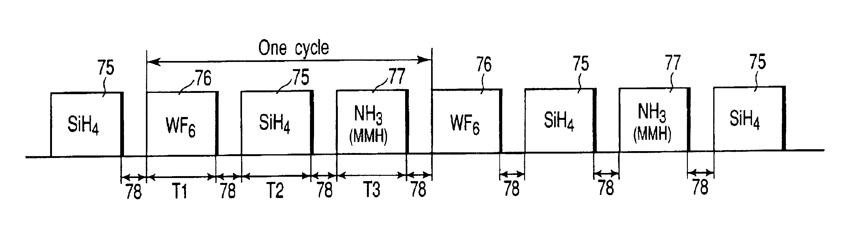
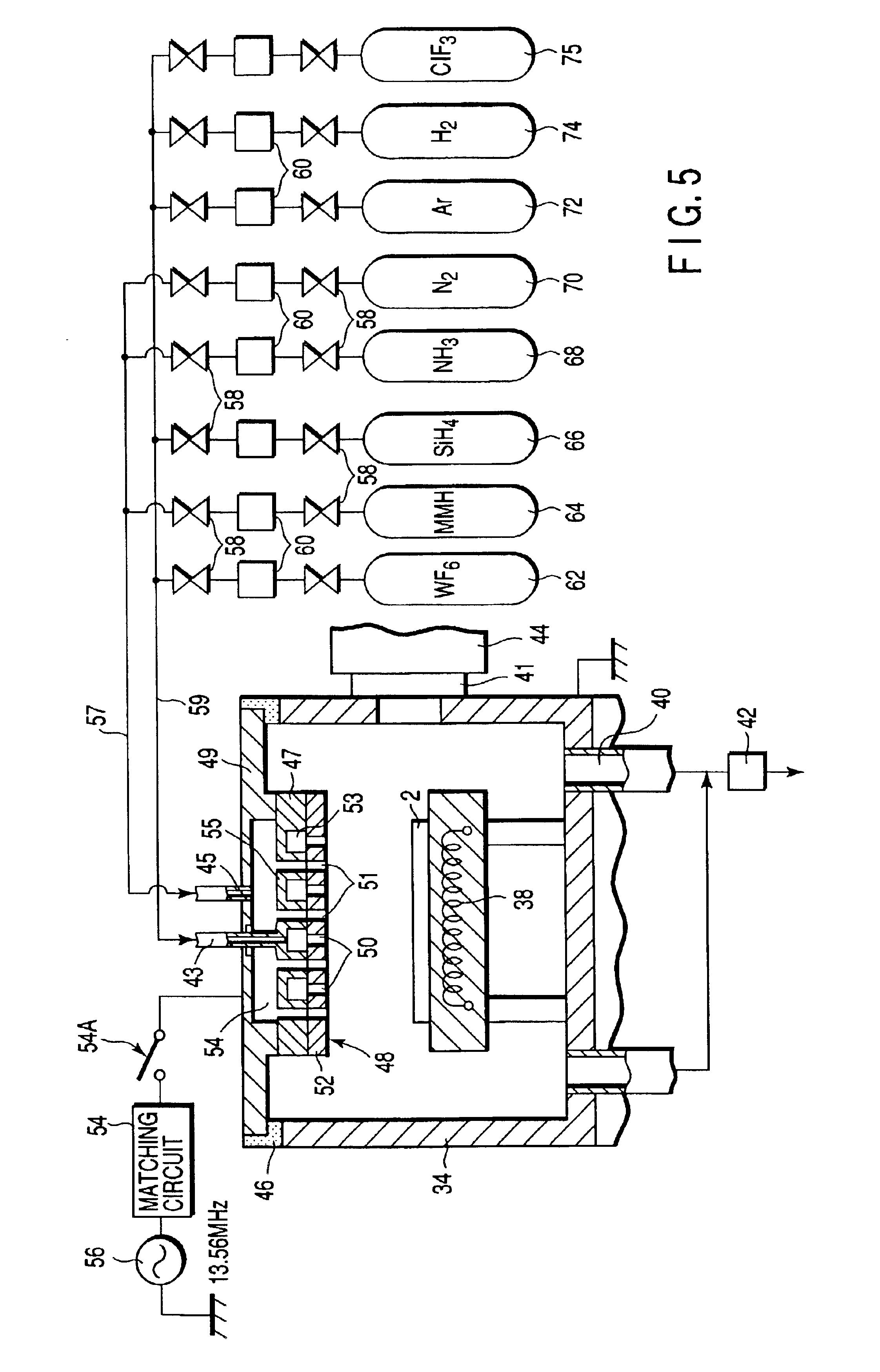
Now, embodiments of the present invention will be explained with reference to drawings.

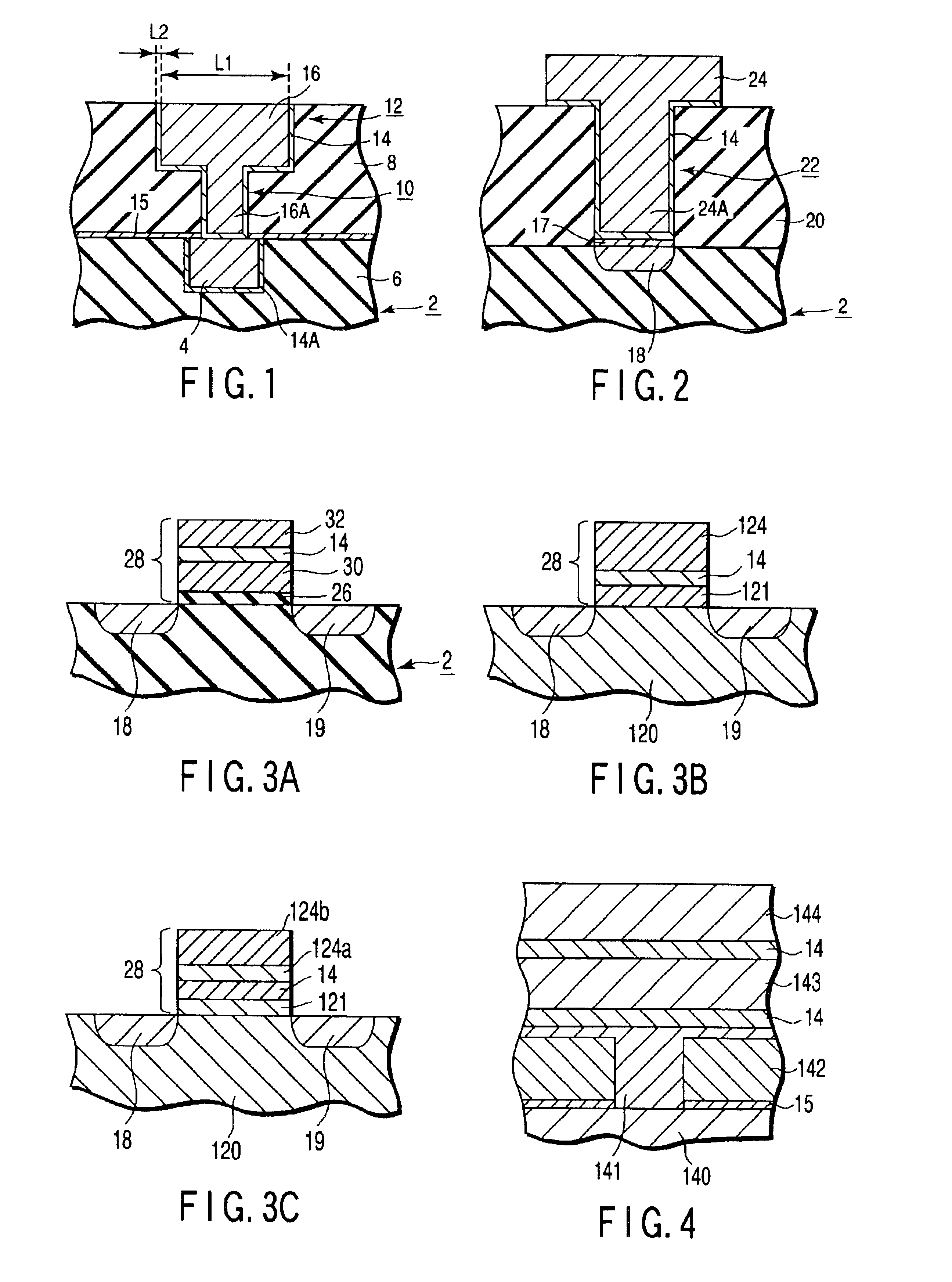
FIG. 1 is an enlarged sectional view showing a barrier metal applied to a Cu dual damascene wiring. FIG. 2 is an enlarged sectional view showing a barrier metal applied to a contact hole. FIGS. 3A to 3C show respectively an enlarged sectional view showing a barrier metal applied to a gate electrode. FIG. 4 is an enlarged sectional view showing a barrier metal applied to a capacitor electrode.

The dual damascene process for forming Cu dual damascene wiring as shown in FIG. 1 is employed for forming a multi-layered structure of wiring so as to attain a high-performance and multi-functional device in a semiconductor integrated device, i.e. a semiconductor integrated circuit. This dual damascene process is featured in that the wirings and via-plugs are simultaneously formed so as to enable an upper wiring layer to be connected with a lower wiring layer, thereby making it possible to reduce the number o...


PUM

PropertyMeasurementUnit
dielectric constantaaaaaaaaaa
width L1aaaaaaaaaa
width L1aaaaaaaaaa

Abstract

There is provided a method of forming a barrier metal which is designed to be interposed between a metal layer and an insulating layer, both constituting a multi-layered structure of semiconductor device, the method comprising the steps of positioning a substrate having the insulating layer formed thereon at a predetermined position inside a processing vessel forming a processing space, and alternately introducing a gas containing a refractory metallic atom, a gas containing Si atom and a gas containing N atom into the processing vessel under a predetermined processing pressure, thereby allowing a refractory metal nitride or a refractory metal silicon nitride to be deposited on the insulating layer by way of atomic layer deposition.

Description

BACKGROUND OF THE INVENTION1. Field of the InventionThe present invention relates to a method of forming a barrier film and to a method of forming the wiring structure and electrodes of semiconductor device having a barrier film.2. Description of the Related ArtGenerally, in the manufacture of a semiconductor integrated device such as a semiconductor integrated circuit, various processes such as film-formation, oxidative diffusion and etching are repeatedly applied onto a semiconductor wafer to form a large number of transistor, capacitors and resistance, and thereafter these elements are connected with each other through wiring patterns. Furthermore, in order to meet persistent demands for a high-performance integrated circuit as well as for a multi-functional integrated circuit, it is now required to further reduce the line width of wiring patterns and to further enhance the integration of the semiconductor elements. Moreover, a multi-layered structure has come to be employed in w...

Claims


Application Information

Patent Timeline
Patent Type & Authority Patents(United States)
IPC IPC(8): H01L21/285H01L23/52H01L21/70H01L21/02H01L21/28H01L23/532H01L21/768H01L29/40H01L29/49
CPCH01L21/28061H01L21/28556H01L21/28568H01L21/76843H01L21/76877H01L23/53238H01L29/4941H01L2924/0002H01L2924/00
Inventor MATSUSE, KIMIHIROOTSUKI, HAYASHI
Owner TOKYO ELECTRON LTD
Why Eureka
Try Eureka