

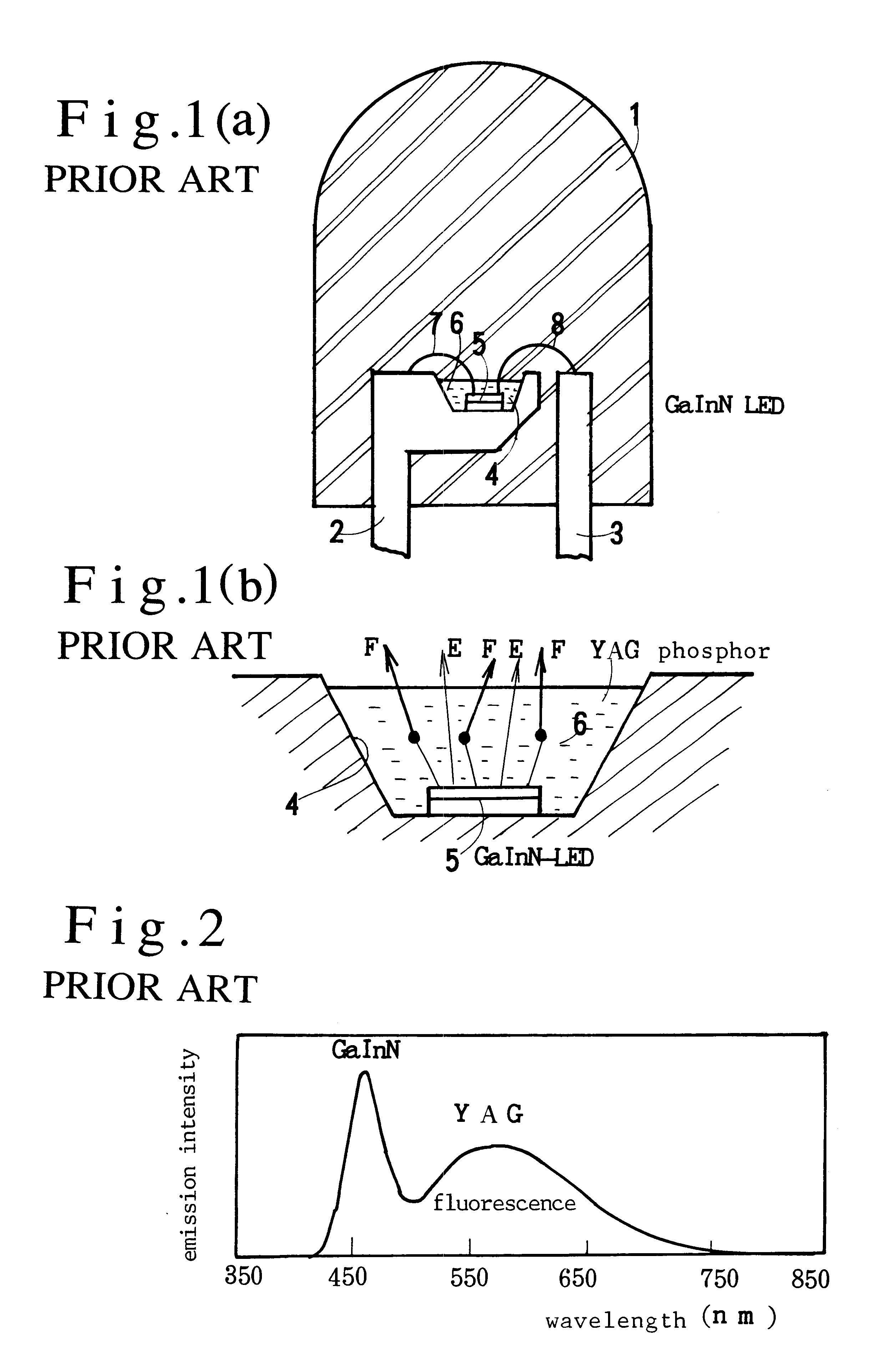
White color light emitting diode and neutral color light emitting diode
a light-emitting diode and white color technology, applied in the direction of discharge tube/lamp details, discharge tube luminescnet screens, electric discharge lamps, etc., can solve the problems of short life of incandescent light bulbs, low luminous efficiency, and inability to replace all current light sources of monochromatic leds, so as to accelerate the yield of fluorescence, reduce production costs and stem costs, and reduce material costs
- Summary
- Abstract
- Description
- Claims
- Application Information
AI Technical Summary
Benefits of technology
Problems solved by technology
Method used
Image

Examples
embodiment 2 (
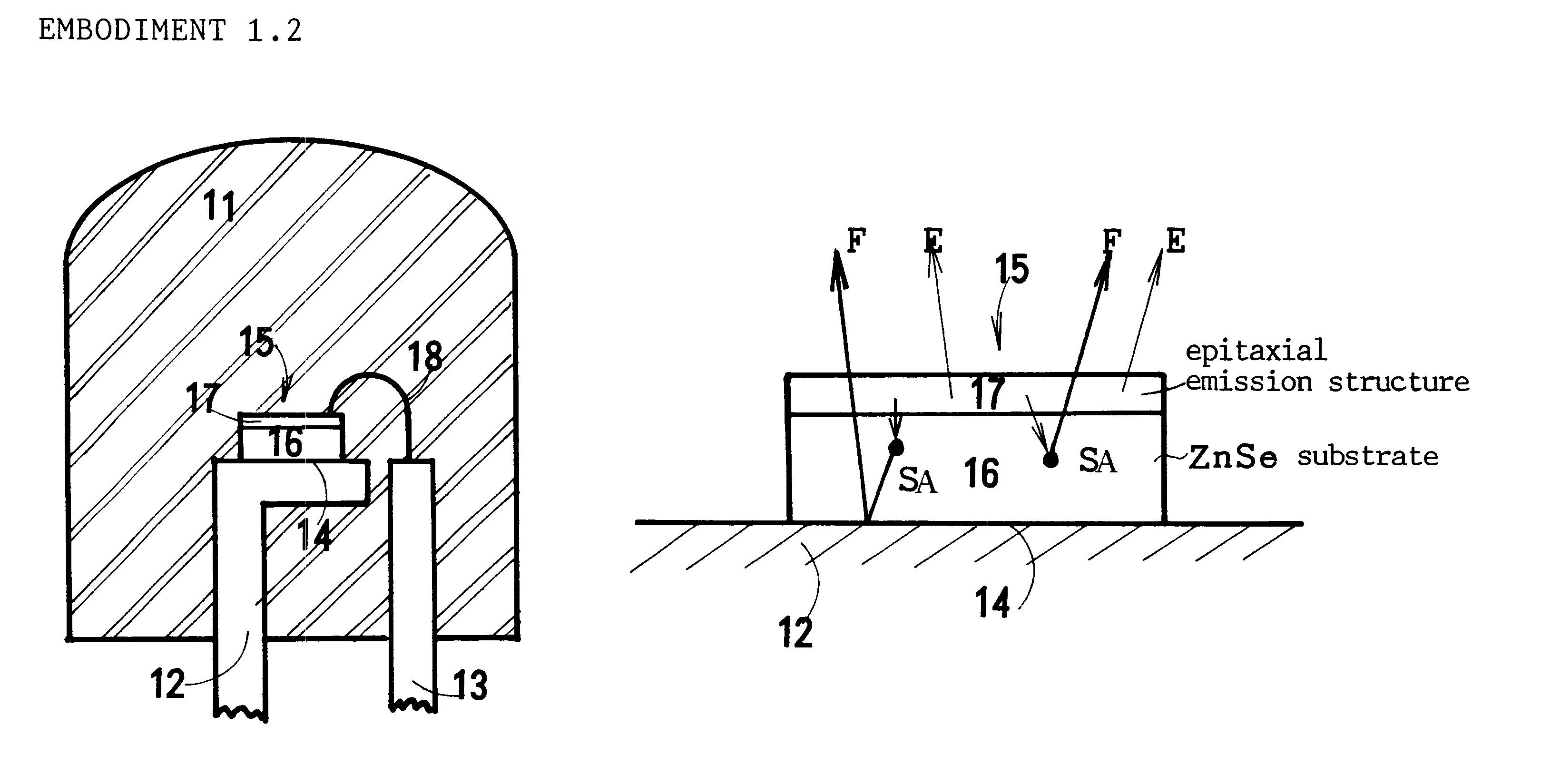
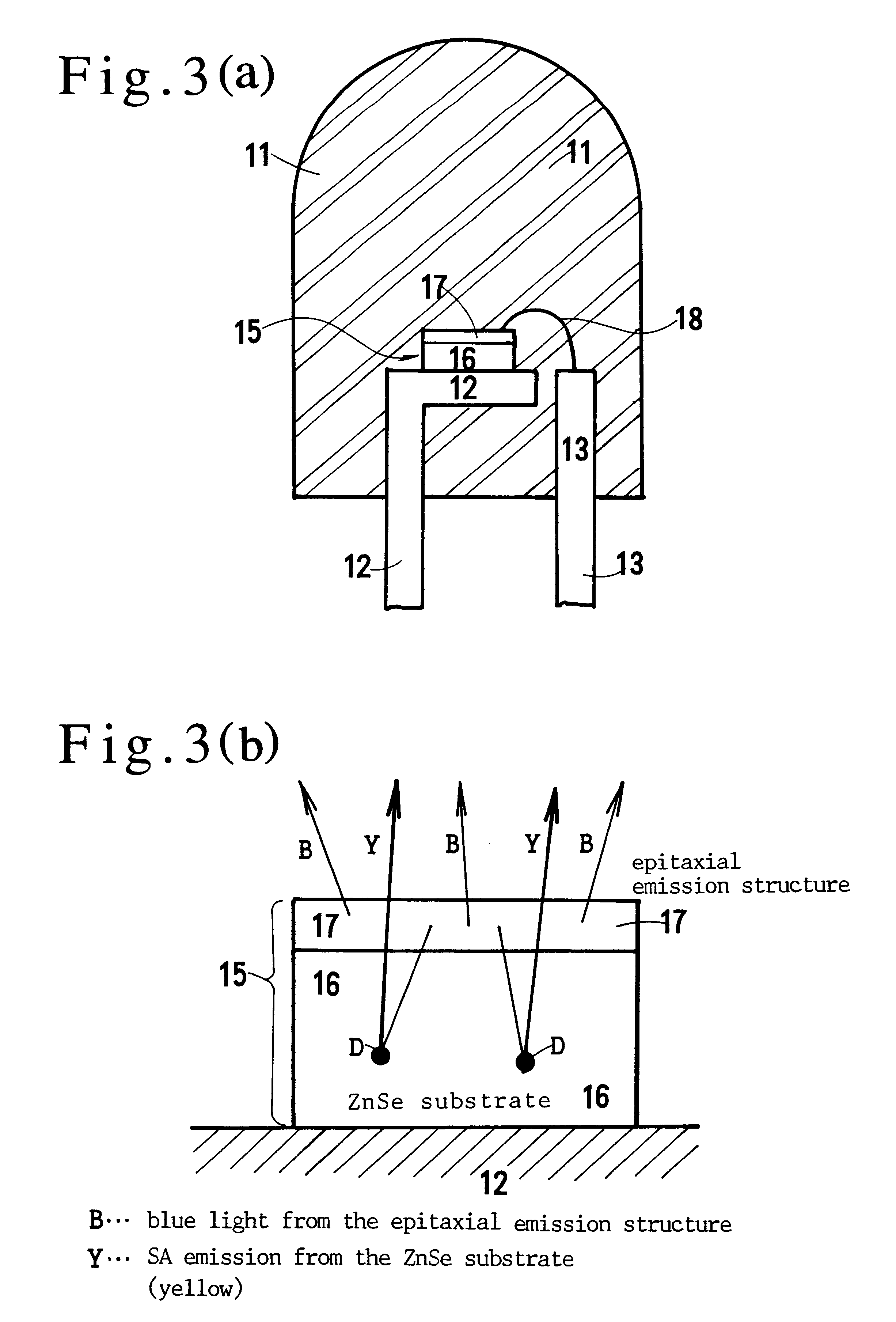
[EMBODIMENT 2 (Grain-growth ZnSe substrate, single quantum well or double hetero active layer, normal posture)
The former embodiment started from the CVT (Chemical Vapor Transport=iodine transport)-made ZnSe substrate. There is another growing method called grain-growth method for the growth of a ZnSe single crystal. The grain-growth method utilizes neither chemical reaction nor transportation. The grain-growth method converts a polycrystal ZnSe to a single crystal ZnSe by heating a part of the polycrystal for facilitating the movement of grain walls in the polycrystal, and inducing the enlargement of a single grain size. Small grains move, rotate to the same orientation as the dominant grain, and merge to the dominant grain together. Finally, all the grains are unified into a single grain by the annealing. Dispensing with iodine (I) as a carrier of Zn, the grain-growth method can make a purer ZnSe single crystal. The ZnSe crystal is cut into thin ZnSe wafers. Aluminum is doped to th...
embodiment 3 (
[EMBODIMENT 3 (Al-doped grain-growth ZnSe; ZnSe active layer; reverse posture, three thicknesses of 100 .mu.m, 300 .mu.m and 700 .mu.m)
An Al-doped ZnSe single crystal is produced by the grain-growth method. The ZnSe crystal is cut into a 300 .mu.m thick wafer and a 700 .mu.m thick wafer. The wafers are annealed. The carrier (electron) density is heightened to about 5.times.10.sup.17 cm.sup.-3 to 1.times.10.sup.18 cm.sup.-3. An epitaxial film structure of FIG. 8 similar to embodiment 1 is formed on the Al-doped ZnSe wafer by the MBE apparatus of FIG. 15. The epitaxial film strata of embodiment 3 are,
(1) n-type ZnSe substrate 62 (Al-dope; 300 .mu.m thick and 700 .mu.m thick)
(2) n-type ZnSe buffer layer 63 (Cl-dope)
(3) n-type Zn.sub.0.85 Mg.sub.0.15 S.sub.0.10 Se.sub.0.90 cladding layer 64 (Cl-dope)
(4) multiquantum well active layer 65=five fold strata of a unit of a 10 nm thick ZnSe film and a 5 nm thickZn.sub.0.88 Cd.sub.0.12 Se film
(5) p-type Zn.sub.0.85 Mg.sub.0.15 S.sub.0.10 Se.su...
embodiment 4 (
[Embodiment 4 (Reverse posture, reflection plane, ZnSe / ZnCdSe active layer)]
PUM
 Abstract
Description
Claims
Application Information