Method for Growth of Gan Single Crystal, Method for Preparation of Gan Substrate, Process for Producing Gan-Based Element, and Gan-Based Element

a technology of gan single crystal and gan-based elements, which is applied in the direction of crystal growth process, polycrystalline material growth, chemically reactive gas growth, etc., can solve the problems of increasing the unit cost of production, difficult element processing, and deterioration of element characteristics, so as to improve the performance of gan-based elements and improve the fabrication steps of gan-based elements. , the effect of low d

Inactive Publication Date: 2008-10-23
FURUKAWA COMPANY +4
View PDF6 Cites 240 Cited by
  • Summary
  • Abstract
  • Description
  • Claims
  • Application Information

AI Technical Summary

Benefits of technology

[0036]The arrangement of the present invention can grow a low-defect, high-quality GaN-based thin film (thick film) by using a metal buffer layer on a substrate made of a different kind of single crystal, a polycrystal, an amorphous semiconductor, or a metal. This GaN-based thin film (thick film) can be formed as an n-type, p-type, or undoped film.
[0037]Since a GaN template substrate including a metal buffer layer can be fabricated, a light emitting element (e.g., a light emitting diode or laser diode) or electronic element can be fabricated on the substrate.
[0038]It is also possible to fabricate a high-output, high-luminance light emitting diode by reflection of the metal buffer layer.
[0039]The GaN-based element fabrication method of the present invention makes it possible not only to improve the performance of a GaN-based element, but also to greatly improve the GaN-based element fabrication steps, thereby largely reducing the GaN-based element fabrication cost.
[0040]Since a GaN GaN freestanding substrate is fabricated by selective chemical etching of a metal buffer layer or / and a metal nitride layer, it is possible to greatly improve the fabrication process after lift-off, thereby increasing the throughput and largely reducing the fabrication process cost.

Problems solved by technology

However, a large lattice mismatching and a large thermal expansion coefficient difference cause a high defect density, that is, a dislocation density of about 1010 / cm2, thereby posing many problems such as element characteristic deterioration and the difficulty in element processing caused by the chemical resistance characteristic.
However, these growth techniques increase the unit cost of production because a number of steps are necessary to fabricate a substrate before the growth, and also have problems in reproducibility and yield.
As described above, the flip-chip technique, the use of the patterned sapphire substrate, the technique that increases the efficiency by using a reflecting electrode metal, and the like have been proposed to fabricate high-luminance, blue and ultraviolet light emitting diodes and laser diodes, but various problems such as the complexity of fabrication steps and the inefficiency of production have arisen.
However, even when this buffer layer exists, a large lattice mismatching and a large thermal expansion coefficient difference cause a high defect density, that is, a dislocation density of about 1010 / cm2.
Also, an electrode is difficult to form on the sapphire substrate because the sapphire substrate has an insulation property.
Therefore, complicated steps including a step of dry-etching a grown thin film by about a few μm is necessary to form an electrode for a device.
However, GaN bulk growth is technically difficult in the conventional GaN substrate fabrication.
Since, however, these methods require a high process cost after the growth of the thick GaN film, the development of a low-cost process has been desired.
Unfortunately, even when Cr is stacked on a sapphire substrate, this Cr forms a polycrystalline or multi-domain layer.
A single crystal is difficult to grow on a polycrystalline or multi-domain layer.
The existence of this oxide layer interferes with the growth of a GaN single crystal.
It is of course also possible to stack another metal by sputtering, nitride the metal, and epitaxially grow single-crystal GaN on the nitrided metal, but the above-mentioned difficulties (a metal film stacks as a polycrystalline layer, causes surface oxidation, and makes the formation of a single crystal difficult) still exist.
However, as the references disclose, although a GaN layer is formed after the formation of AlN, Al is unfavorable to the subsequent GaN growth process because the melting point of Al is low as a metal buffer layer (see patent reference 1).
Also, although titanium is used as a metal film to form air spaces in a GaN layer by a Ti film and TiN film and then to detach the GaN layer, the air spaces may deteriorate the crystallinity of the GaN layer (see patent reference 2).

Method used


Image

  • Method for Growth of Gan Single Crystal, Method for Preparation of Gan Substrate, Process for Producing Gan-Based Element, and Gan-Based Element
  • Method for Growth of Gan Single Crystal, Method for Preparation of Gan Substrate, Process for Producing Gan-Based Element, and Gan-Based Element
  • Method for Growth of Gan Single Crystal, Method for Preparation of Gan Substrate, Process for Producing Gan-Based Element, and Gan-Based Element

Examples


Embodiment Construction

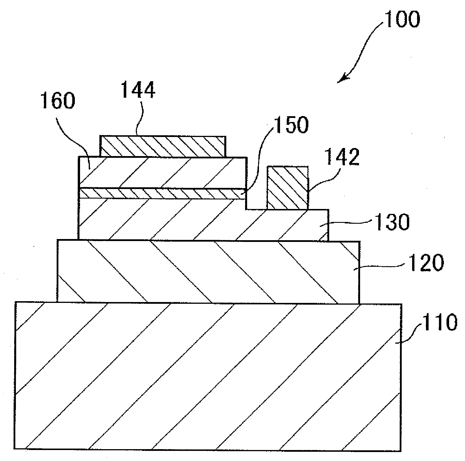
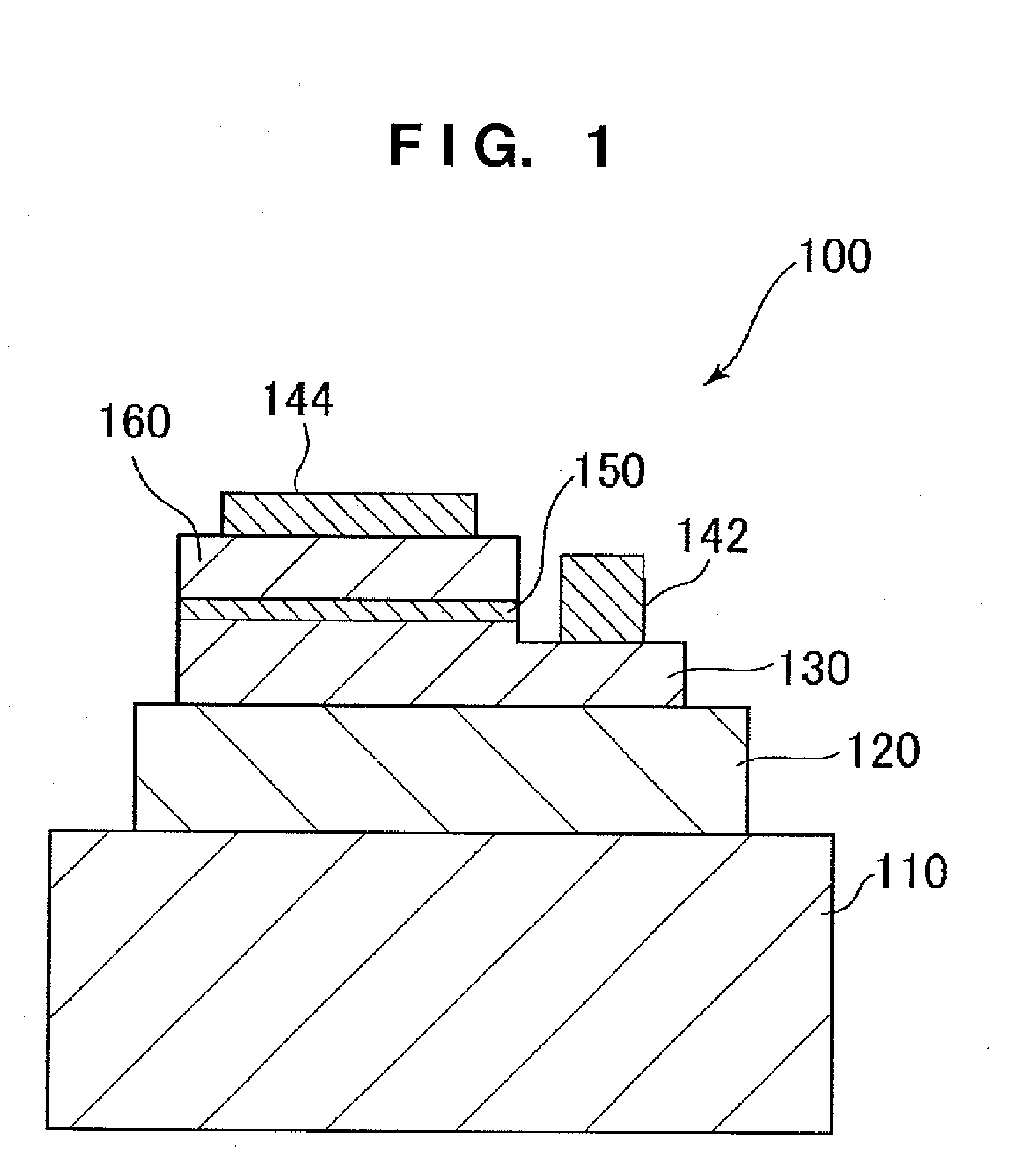
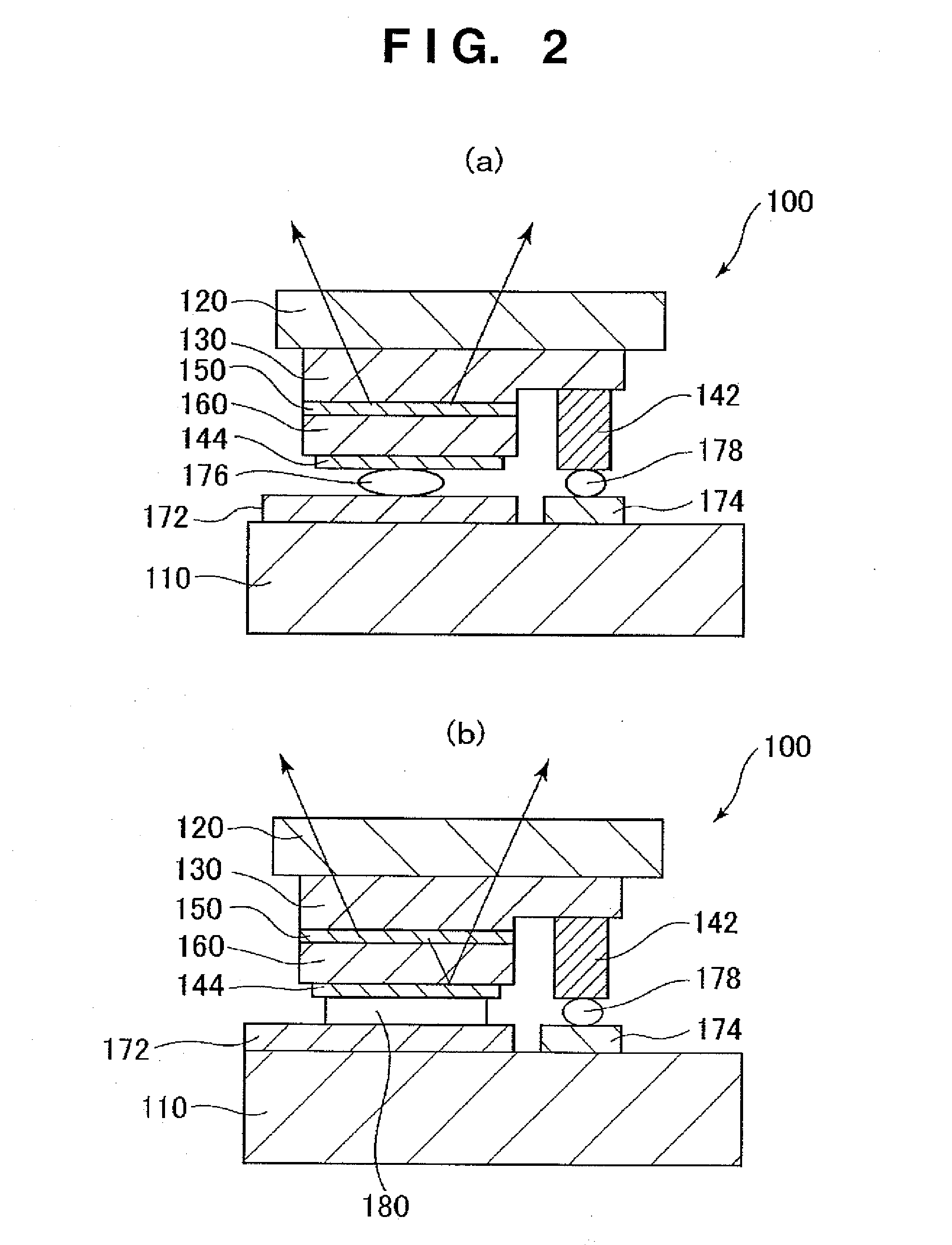
[0102]The present invention forms a metal buffer layer on a different kind of single-crystal substrate, a polycrystalline substrate, an amorphous substrate, or a metal substrate, in addition to a sapphire substrate and SiC substrate, by electron beam evaporation method (E-beam evaporator), thermal evaporation method (Thermal evaporator), sputtering method (Sputter), chemical vapor deposition method (Chemical Vapor Deposition), or metal organic chemical vapor deposition (MOCVD), and then grows single-crystal GaN on the metal buffer layer. It is the first attempt to use a metal as a buffer layer on various substrates, and fabricate a light emitting element or electronic element on the metal buffer layer. This makes it possible to provide various structures and various substrates of GaN-based light emitting elements in the future. Since the metal buffer layer is inserted in the interface between any of various substrates such as a sapphire substrate or SiC substrate and a GaN-based sin...


PUM

PropertyMeasurementUnit
temperatureaaaaaaaaaa
thicknessaaaaaaaaaa

Abstract

A GaN-based thin film (thick film) is grown using a metal buffer layer grown on a substrate. (a) A metal buffer layer (210) made of, for example, Cr or Cu is vapor-deposited on a sapphire substrate (120). (b) A substrate obtained by vapor-depositing the metal buffer layer (210) on the sapphire substrate (120) is nitrided in an ammonia gas ambient, thereby forming a metal nitride layer (212). (c) A GaN buffer layer (222) is grown on the nitrided metal buffer layers (210, 212). (d) Finally, a GaN single-crystal layer (220) is grown. This GaN single-crystal layer (220) can be grown to have various thicknesses depending on the objects. A freestanding substrate can be fabricated by selective chemical etching of the substrate fabricated by the above steps. It is also possible to use the substrate fabricated by the above steps as a GaN template substrate for fabricating a GaN-based light emitting diode or laser diode.

Description

TECHNICAL FIELD[0001]The present invention relates to the fabrication of a GaN freestanding substrate or GaN template substrate and a method of fabricating a GaN-based element using the GaN template substrate and including a light-emitting element such as a light-emitting diode or laser diode or an electronic element and, more particularly, to the fabrication of a high-efficiency light emitting element or the like performed by a GaN single crystal growth method using a metal buffer layer.BACKGROUND ART[0002]Nichia Corporation, Japan and Lumi LED, U.S.A. are going ahead in the fields of the development and production of blue and white light emitting diodes and laser diodes using GaN-based compound semiconductors. Recently, various high-luminance light emitting element structures to be applied to the fields of illumination such as household fluorescent lamps and LCD (Liquid Crystal Display) backlights have been proposed and produced. GaN-based materials have well exhibited their possi...

Claims


Application Information

Patent Timeline
Patent Type & Authority Applications(United States)
IPC IPC(8): H01L21/30H01L31/20H01L33/12H01L33/32
CPCC30B25/02C30B25/183C30B29/406H01L21/0237H01L21/02458H01L21/02488H01L21/02491H01L21/02502H01L21/0254H01L21/02614H01L29/2003H01L33/007H01L33/12
Inventor YAO, TAKAFUMICHO, MEOUNG-WHAN
Owner FURUKAWA COMPANY
Why Eureka
Try Eureka