Protected Solder Ball Joints in Wafer Level Chip-Scale Packaging

a technology of wafer level and chip scale, applied in the direction of electrical equipment, semiconductor devices, semiconductor/solid-state device details, etc., can solve the problems of too short lead wire pitch, cracks between the solder ball and the electrode post, and limitations in the mounting of the packaged chip board, so as to increase the strength and reliability of the solder ball joint, increase the strength and reliability of the solder joint, and reduce the effect of im

Active Publication Date: 2009-05-21
TAIWAN SEMICON MFG CO LTD
View PDF86 Cites 97 Cited by
  • Summary
  • Abstract
  • Description
  • Claims
  • Application Information

AI Technical Summary

Benefits of technology

[0015]An advantage of a preferred embodiment of the present invention is an increased strength and reliability of the solder ball joint. Because the joint is located below the buffer layer, it is protected from direct outside contact.
[0016]A further advantage of a preferred embodiment of the present invention is the protection of copper electrodes. In embodiments where the electrode posts are formed using copper, the capping layer protects the copper from oxidizing.
[0017]An additional advantage of a preferred embodiment of the present invention configured with multi-column electrodes is an incre

Problems solved by technology

However, increased pin count peripherally designed and arranged around the package typically results in too short of a pitch of lead wire, yielding limitations in board mounting of the packaged chip.
Although, these advances have allowed for miniaturization in electronic devices, the ever-demanding trend toward even smaller, lighter, and thinner consumer products have prompted even further attempts at package miniaturization.
One disadvantage of current WLCSP technology is the formation of cracks between the solder ball and the electrode post.
As a result, a relatively large stress derived from this difference is exhibited on the joint between the post and the bump electrode, which often causes cracks to form in the bonding area between the bump electrode/post and the solder ball or bump.
This exposure makes the solder ball more susceptible to physical impact, and places the more vulnerable joint in an exposed position as well.
Because the weld joint is so small in WLCSP, cracks, such as crack 104, may form more easily under the stress

Method used


Image

  • Protected Solder Ball Joints in Wafer Level Chip-Scale Packaging
  • Protected Solder Ball Joints in Wafer Level Chip-Scale Packaging
  • Protected Solder Ball Joints in Wafer Level Chip-Scale Packaging

Examples


Embodiment Construction

[0028]The making and using of the presently preferred embodiments are discussed in detail below. It should be appreciated, however, that the present invention provides many applicable inventive concepts that can be embodied in a wide variety of specific contexts. The specific embodiments discussed are merely illustrative of specific ways to make and use the invention, and do not limit the scope of the invention.

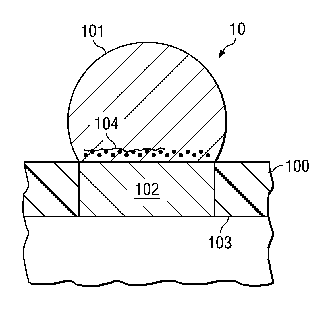
[0029]With reference now to FIG. 2, there is shown a cross-sectional view of WLCSP feature 20 configured according to one embodiment of the present invention. Wafer 200 includes electrode post 201 formed thereon. Insulating layer 202 is formed on top of wafer 200 and surrounds electrode post 201. During the manufacturing process, electrode post 201 was flush at the top with the top of insulating layer 202. Electrode post 201 is etched back below the level of insulating layer 202. In a preferred embodiment, no extra photoresist layer is used during the etching process because ...


PUM


Abstract

Protection of a solder ball joint is disclosed in which the solder ball joint is located below the surface level of the encapsulating buffer layer. The buffering layer is etched to expose one or more electrode posts, each of which may be made up of a single column or multiple columns. A top layer resulting either from a top conductive cap or a plating layer around the electrode posts also lies below the buffer layer. When the solder ball is placed onto the posts, the solder/ball joint is protected in a position below the surface of the buffer layer, while still maintaining an electrical connection between the various solder balls and their associated or capping/plating material, electrode posts, wiring layers, and circuit layers. Therefore, the entire ball joint is protected from direct stress.

Description

TECHNICAL FIELD[0001]The present invention relates generally to wafer level chip scale packaging (WLCSP), and more particularly to enhancing the reliability of solder ball joints in WLCSP.BACKGROUND[0002]The past few decades have seen many shifts in electronics and semiconductor packaging that have impacted the entire semiconductor industry. The introduction of surface-mount technology (SMT) and ball grid array (BGA) packages were generally important steps for high-throughput assembly of a wide variety of integrated circuit (IC) devices, while, at the same time, allowing reduction of the pad pitch on the printed circuit board. Conventionally packaged ICs have a structure basically interconnected by fine gold wire between metal pads on the die and electrodes spreading out of molded resin packages. Dual inline package (DIP) and quad flat package (QFP) are fundamental structures of current IC packaging. However, increased pin count peripherally designed and arranged around the package ...

Claims


Application Information

Patent Timeline
IPC IPC(8): H01L21/441
CPCH01L23/49816H01L24/03H01L2924/0002H01L2924/00014H01L2224/11334H01L2224/04042H01L2224/48647H01L2924/01006H01L2924/00013H01L2224/13027H01L2224/05571H01L2224/13005H01L2924/14H01L2924/014H01L2924/01327H01L2924/01082H01L2924/01079H01L2924/01078H01L2924/01075H01L2924/01074H01L2924/0105H01L24/05H01L24/11H01L24/12H01L2224/0231H01L2224/02313H01L2224/0401H01L2224/05569H01L2224/056H01L2224/05647H01L2224/1132H01L2224/1147H01L2224/1148H01L2224/11901H01L2224/13022H01L2224/131H01L2224/16H01L2224/45144H01L2924/01013H01L2924/01015H01L2924/01028H01L2924/01029H01L2924/01033H01L2924/207H01L2224/13099H01L2924/00H01L2224/05552H01L2924/351H01L2924/181H01L2224/05008H01L2224/13023H01L2224/02351H01L24/13
Inventor WANG, CHUNG YULEE, CHIEN-HSIUNTSAO, PEI-HAWCHANG, KUO-CHINLIN, CHUNG-YIKIANG, BILL
Owner TAIWAN SEMICON MFG CO LTD
Why Eureka
Try Eureka