Photovoltaic element and method for manufacture thereof

a photovoltaic element and photovoltaic technology, applied in the direction of pv power plants, solid-state devices, semiconductor devices, etc., can solve the problems of reducing conversion efficiency, degrading the characteristic of heterojunction interfaces, and increasing doping, so as to eliminate the lowering of open circuit voltage and short circuit, and improve the output characteristic of photovoltaic elements.

Inactive Publication Date: 2001-03-27
SANYO ELECTRIC CO LTD
View PDF18 Cites 105 Cited by
  • Summary
  • Abstract
  • Description
  • Claims
  • Application Information

AI Technical Summary

Benefits of technology

An alkaline solution containing an interface active agent is preferably used in the second process. In the above composition, the appearance of the surface after isotropically etched does not affect the strength of the short circuit current of a photovoltaic element since the bottoms of the uneven sections are slightly rounded. And the variety of the thickness of the amorphous or micro crystalline layer is prevented, eliminating the lowered open circuit voltage and short circuit between the substrate and the electrode. Therefore, it is possible to achieve an improved output characteristic of a photovoltaic element and high yields.

Problems solved by technology

In the amorphous silicon layer or mircocrystalline silicon layer which is doped, however, defects caused by doping increase and the characteristic of the heterojunction interface is degraded.
The degradation of the interface characteristic results in a lower conversion efficiency because of a recombination of carriers in the case where these silicon layers are used for a photovoltaic element.
In the above described conventional structure of the front surface of the substrate 1, a problem may occur when the intrinsic amorphous silicon layer 2 is formed on the substrate 1 by a plasma CVD method.

Method used


Image

  • Photovoltaic element and method for manufacture thereof
  • Photovoltaic element and method for manufacture thereof
  • Photovoltaic element and method for manufacture thereof

Examples


second embodiment

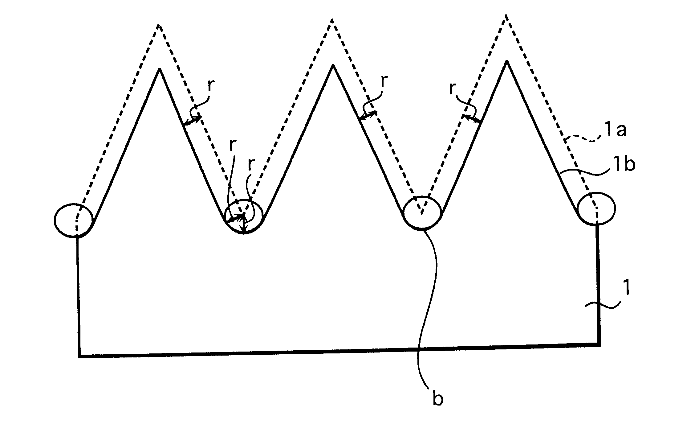
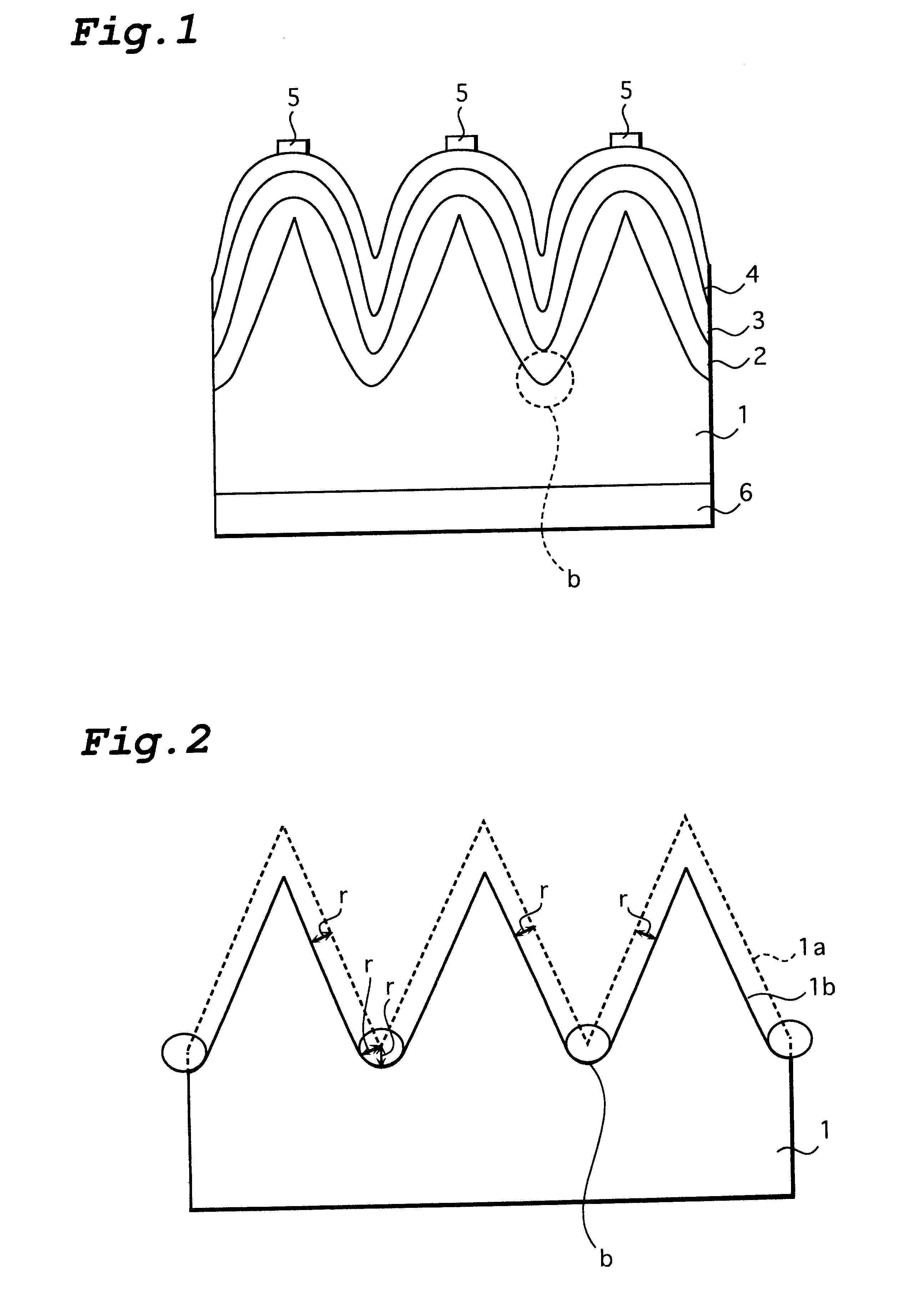
FIG. 4 is a cross sectional view illustrating the present invention. In this embodiment, a BSF (Back Surface Field) type photovoltaic element in which an internal electric field is introduced on the back surface of the substrate 1 to prevent an effect from the recombination of carriers near the back surface of the substrate 1. An n-type high doping layer 7 is formed on the back surface of the n-type substrate 1 as in FIG. 4.

The photovoltaic element in FIG. 4 can be formed by the following processes for example. An n-type crystalline silicon substrate 1 which is sliced along (100) surface and of which resistivity is 0.1-10 .OMEGA.cm and of which thickness is 200-400 .mu.m is prepared. As a first process, the substrate 1 is dipped into a 5 wt. % aqueous solution of sodium hydroxide (NaOH) about 85.degree. C. for ten minutes to remove deformation on the surface of the substrate 1. As a second process, the substrate 1 is dipped into a mixed solution containing 1.5 wt. % aqueous solution...

third embodiment

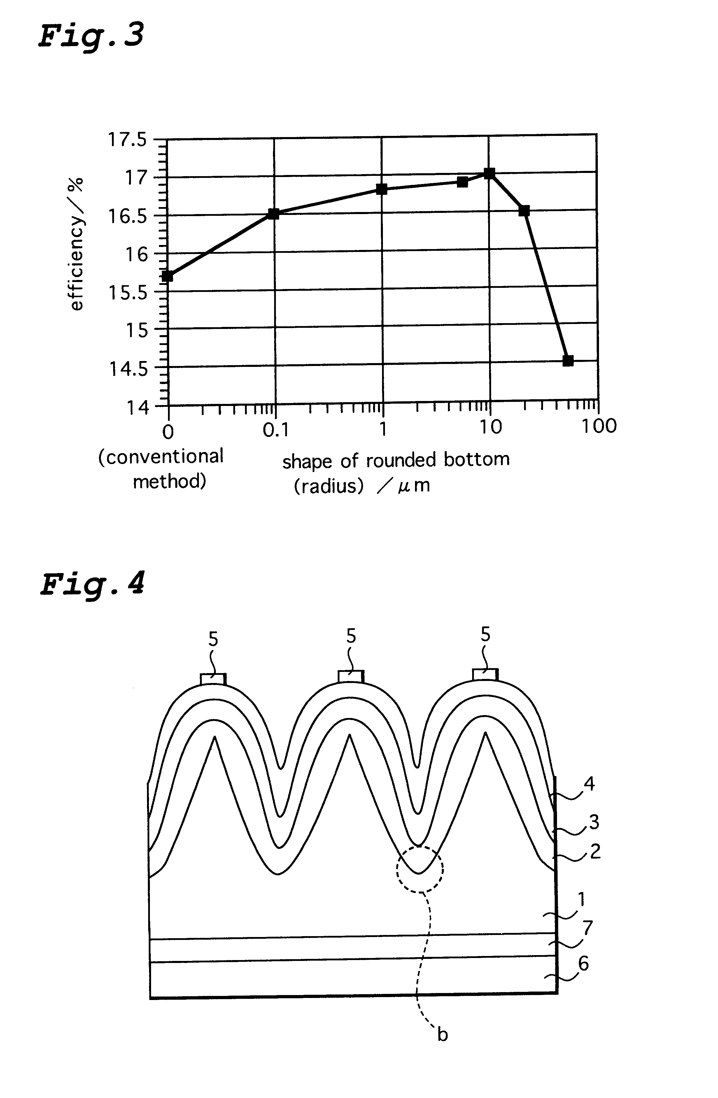
As shown in FIG. 6 of the third embodiment, an intrinsic amorphous silicon layer 2 and a p-type amorphous silicon layer 3 are formed on the front surface of the substrate 1 having uneven sections by a plasma CVD method. A front electrode 4 containing ITO of 1000 .ANG. in thick is formed by sputtering on the p-type amorphous silicon layer 3. A comb-like collecting electrode 5 containing silver is formed by screen printing using Ag paste on the front electrode 4. A back electrode 6 of about 20-25 .mu.m in thick is formed on the back surface of the substrate 1 by using Al paste.

It is convenient to form a back electrode 6 on the whole back surface of the substrate 1 by screen printing using Al paste from the viewpoint of mass production. In this method, a back electrode 6 containing Al of about 20 .mu.m in thick is formed by pasting Al paste on the whole back surface of the substrate 1 by screen printing and calcinating the paste by approximately 700.degree. C. heat treatment.

Recently, ...

fifth embodiment

FIG. 8 of the fifth embodiment illustrates a BSF-type photovoltaic element manufactured in a low-temperature process without using thermal diffusion. An intrinsic amorphous silicon layer 10 of 50-100 .ANG. in thick is deposited on the back surface of the substrate 1 by a plasma CVD method of low-temperature process using silane (SiH.sub.4) where the temperature of the substrate is about 170.degree. C. A high doping n-type amorphous silicon layer 11 of 50-500 .ANG. in thick is deposited on the intrinsic amorphous silicon layer 10 by using silane (SiH.sub.4) and phospine (PH.sub.3)as a dopant gas. A transparent electrode on a back surface 12 containing ITO of 1000 .ANG. in thick is formed by sputtering. A comb-like collecting electrode 9 is formed on the transparent electrode on a back surface 12 by using Ag paste. By these processes, a substantially intrinsic amorphous silicon is interposed between the crystalline silicon substrate and the amorphous silicon layer on the back surface ...


PUM


Abstract

A photovoltaic element which directly converts an optical energy such as solar light into an electric energy. After many uneven sections are formed on the surface of an n-type crystalline silicon substrate (1), the surface of the substrate (1) is isotropically etched. Then the bottoms (b) of the recessed sections are rounded and a p-type amorphous silicon layer (3) is formed on the surface of the substrate (1) through an intrinsic amorphous silicon layer (2). The shape of the surface of the substrate (1) after isotropic etching is such that the bottoms of the recessed sections are slightly rounded and therefore the amorphous silicon layer can be deposited in a uniform thickness.

Description

This invention is related to a photovoltaic element for directly converting an optical energy such as solar light into an electric energy and a method for manufacturing the same.A heterojunction type photovoltaic element, in which an amorphous silicon layer or a micro crystalline silicon layer are deposited on a single crystalline silicon substrate, is well-known. The heterojunction can have its distinguish function when an impurity is doped on an amorphous silicon layer or a micro crystalline silicon layer.In the amorphous silicon layer or mircocrystalline silicon layer which is doped, however, defects caused by doping increase and the characteristic of the heterojunction interface is degraded. The degradation of the interface characteristic results in a lower conversion efficiency because of a recombination of carriers in the case where these silicon layers are used for a photovoltaic element.To overcome this problem, Japanese Patent Laid-Open No. 70183 / 1991 (IPC:H01L 31 / 04) has p...

Claims


Application Information

Patent Timeline
Patent Type & Authority Patents(United States)
IPC IPC(8): H01L31/0352H01L31/0248H01L31/0236H01L21/00H01L25/00H01L31/00
CPCH01L31/035281H01L31/03529H01L31/02363Y02E10/50H01L31/0747
Inventor NAKAI, TAKUOTANIGUCHI, HIROYUKIIENAGA, TERUHIKOKADONAGA, YASUO
Owner SANYO ELECTRIC CO LTD
Why Eureka
Try Eureka