
Engineering emission wavelengths in laser and light emitting devices

a technology of light emitting devices and lasers, which is applied in the direction of lasers, semiconductor lasers, solid-state devices, etc., can solve the problems of mainly limited shift of emission wavelength to 530 nm, and efficiency is usually limited to a few percent, and achieves the effect of reducing the efficiency of semiconductor lasers and reducing the cost of lasers

Active Publication Date: 2012-08-14
MASSACHUSETTS INST OF TECH
View PDF6 Cites 2 Cited by
  • Summary
  • Abstract
  • Description
  • Claims
  • Application Information

AI Technical Summary

Benefits of technology

This approach enables efficient light emission at traditionally inaccessible wavelengths, such as true green, within the same material system, reducing fabrication costs and enabling integration of different colors using the same material system.

Problems solved by technology

For InGaN system, shifting the emission wavelength to 530 nm is mainly limited by the difficulty in growing high quality, high indium content materials.
However, the efficiency is usually limited to a few percent. much lower than typical semiconductor lasers.

Method used


Image

  • Engineering emission wavelengths in laser and light emitting devices
  • Engineering emission wavelengths in laser and light emitting devices
  • Engineering emission wavelengths in laser and light emitting devices

Examples


Embodiment Construction

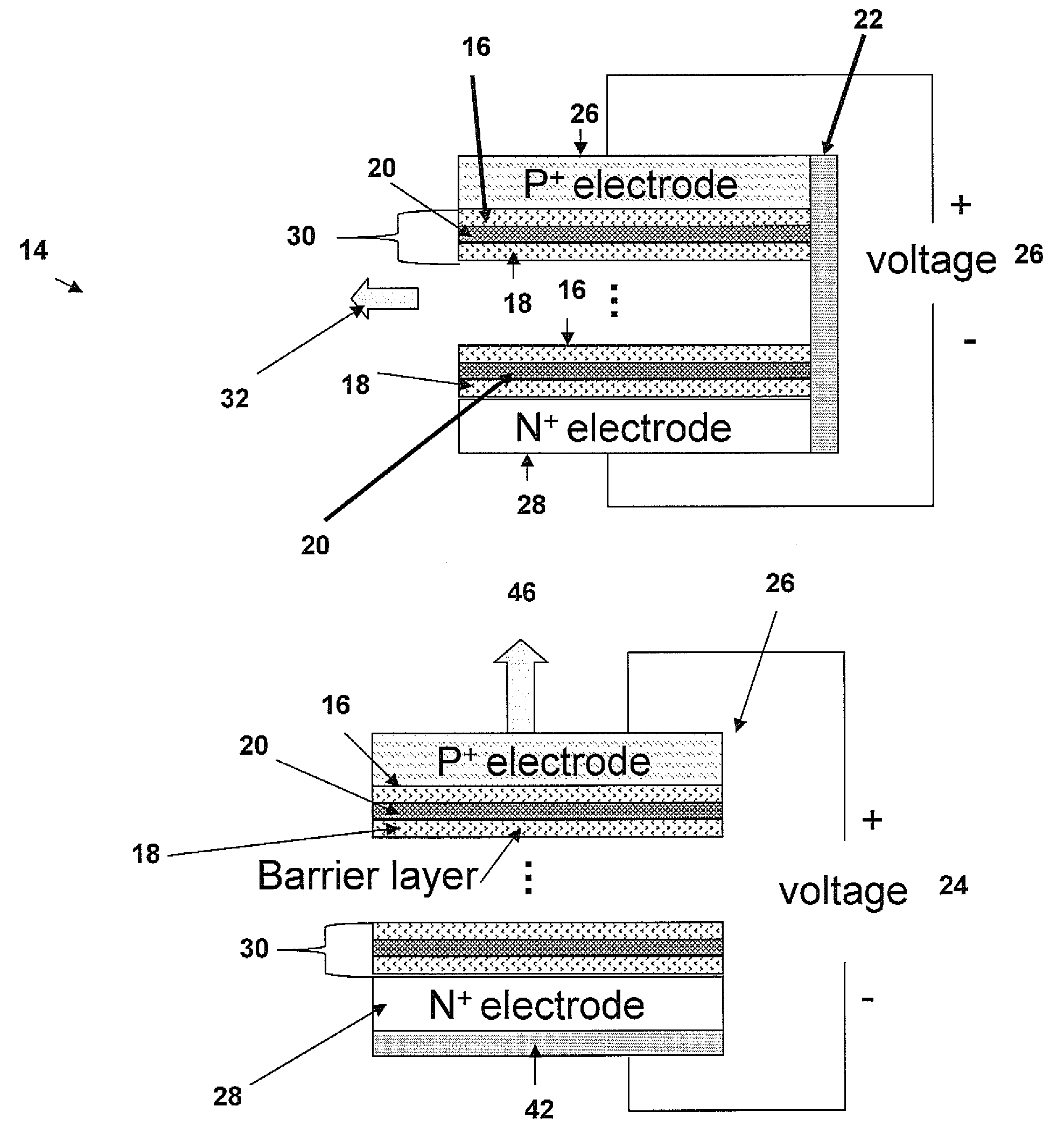
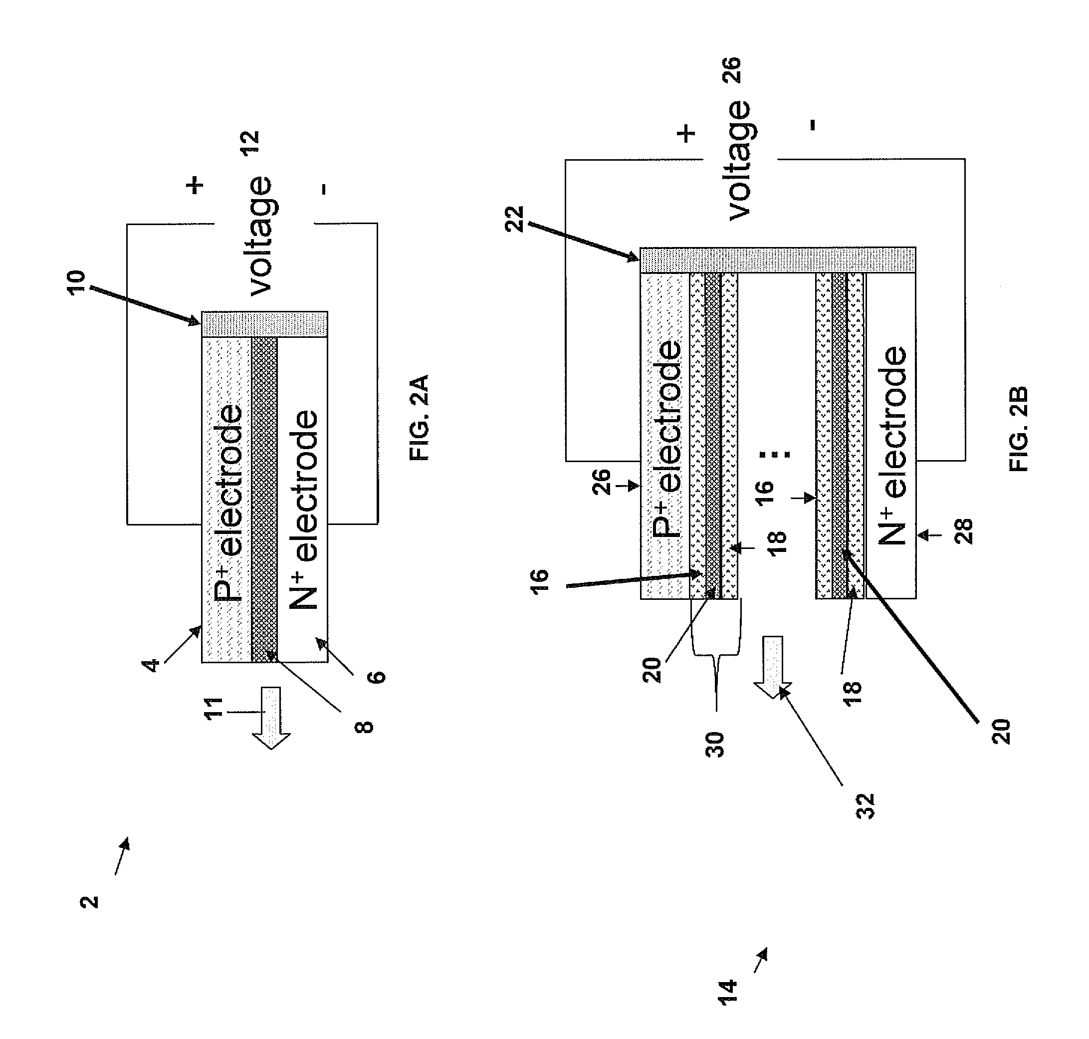
[0008]The invention involves forming novel light emitting devices using indirect bandgap materials. Doped, indirect elemental semiconductor materials, such as germanium, can be engineered as a gain medium for lasing. The invention extends this observation to indirect compound semiconductor materials of various compositions of Al, In, Ga, P, and As for lasing in the wavelength range between 500 nm and 560 nm.

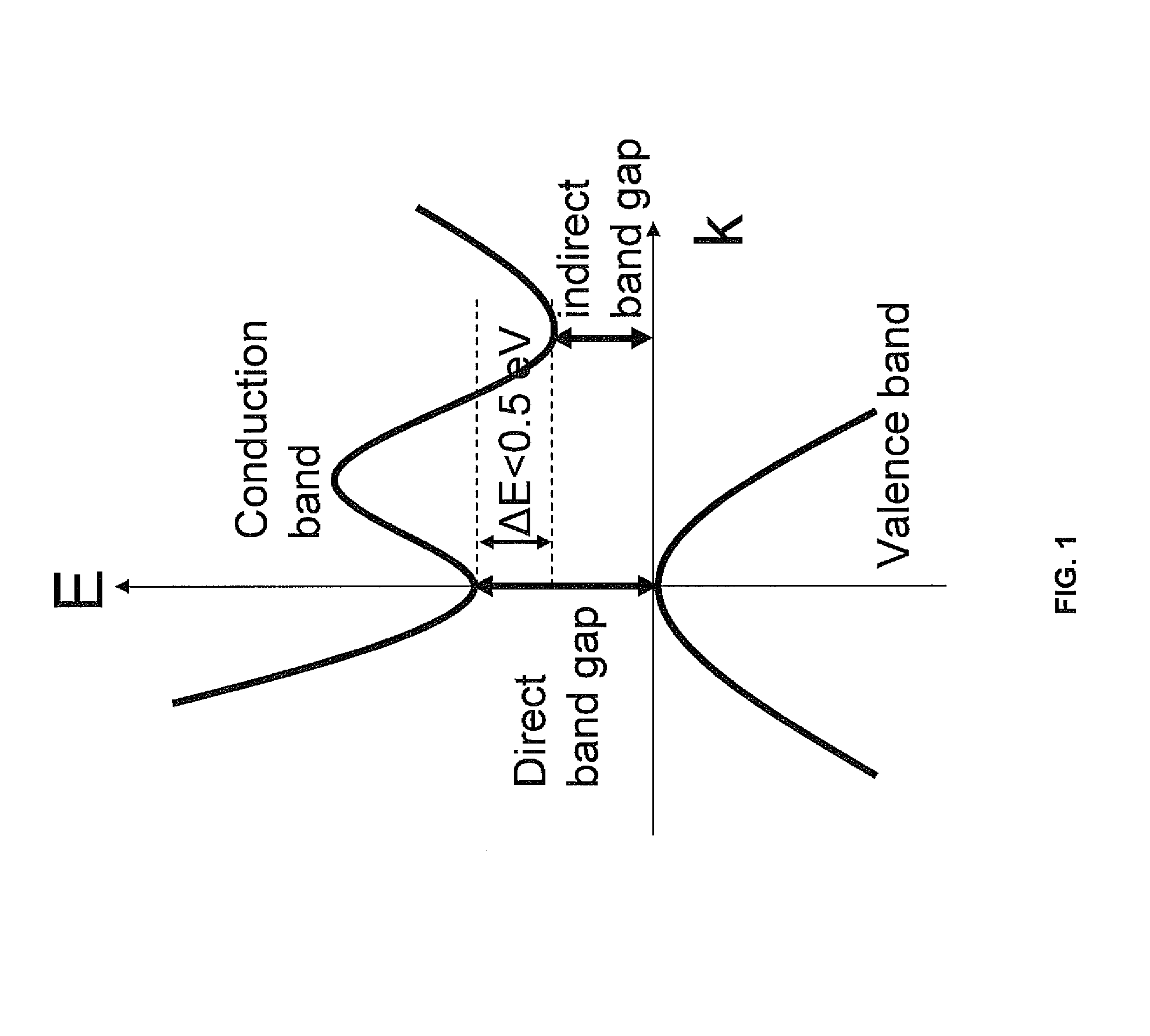
[0009]FIG. 1 shows an energy band diagram of an indirect band gap semiconductor material with an energy difference between the direct and indirect band gaps of less than 0.5 eV, which is defined as a “near-direct gap material” herein. These materials can be band-engineered by strain and n-type doping to achieve light emission at traditionally inaccessible wavelengths. Indirect gap materials are traditionally considered unsuitable for efficient light emitters and lasers due to the low radiative recombination rate. However, if the direct band gap of an indirect gap materials is clo...


PUM


Abstract

A light emitting device is provided that includes at least one first semiconductor material layers and at least one second semiconductor material layers. At least one near-direct band gap material layers are positioned between the at least one first semiconductor layers and the at least one second semiconductor material layers. The at least one first semiconductor layers and the at least one second material layers have a larger band gap than the at least one near-direct band gap material layers. The at least one near-direct band gap material layers have an energy difference between the direct and indirect band gaps of less than 0.5 eV.

Description

BACKGROUND OF THE INVENTION[0001]The invention is related to light emitting devices, and in particular to light emitting devices having indirect bandgap materials.[0002]Truly green semiconductor lasers and LEDs featuring an emission peak wavelength of 530-532 nm, have been a missing component for high quality full color display. InGaN lasers and LEDs emit a bluish-green color at 515 nm, while InGaP lasers and LEDs emit a yellowish-green color at 571 nm. For InGaN system, shifting the emission wavelength to 530 nm is mainly limited by the difficulty in growing high quality, high indium content materials. For InGaP system, tuning the wavelength to 530 nm is limited by a direct-to-indirect gap transition at a Ga content of >72%. Currently, green lasers are achieved by frequency doubling an infrared laser with nonlinear optical materials. However, the efficiency is usually limited to a few percent. much lower than typical semiconductor lasers.SUMMARY OF THE INVENTION[0003]According t...

Claims


Application Information

Patent Timeline
Patent Type & Authority Patents(United States)
IPC IPC(8): H01L29/12
CPCB82Y20/00H01L33/30H01S5/3403H01S5/34333H01L33/06
Inventor KIMERLING, LIONEL C.LIU, JIFENGMICHEL, JURGEN
Owner MASSACHUSETTS INST OF TECH
Learn More