High voltage photovoltaics

Inactive Publication Date: 2018-04-05
IBM CORP
View PDF11 Cites 1 Cited by
  • Summary
  • Abstract
  • Description
  • Claims
  • Application Information

AI Technical Summary

Benefits of technology

The present invention relates to photovoltaic devices that generate power when exposed to light. These devices include a substrate and a layer of P-type material with a first electrode and an N-type layer with a second electrode. The P-type and N-type layers are made from a common base material that has a bandgap of at least 2 electron-volts. The devices can be used for communication functions and can provide power to powered systems like processors and memory. The technical effect of this invention is the generation of power from photovoltaic devices that can be used for communication functions.

Problems solved by technology

This is insufficient for many applications.
However, these solutions may not provide the voltage potentials needed to proficiently run many device operations.

Method used


Image

  • High voltage photovoltaics
  • High voltage photovoltaics
  • High voltage photovoltaics

Examples


Embodiment Construction

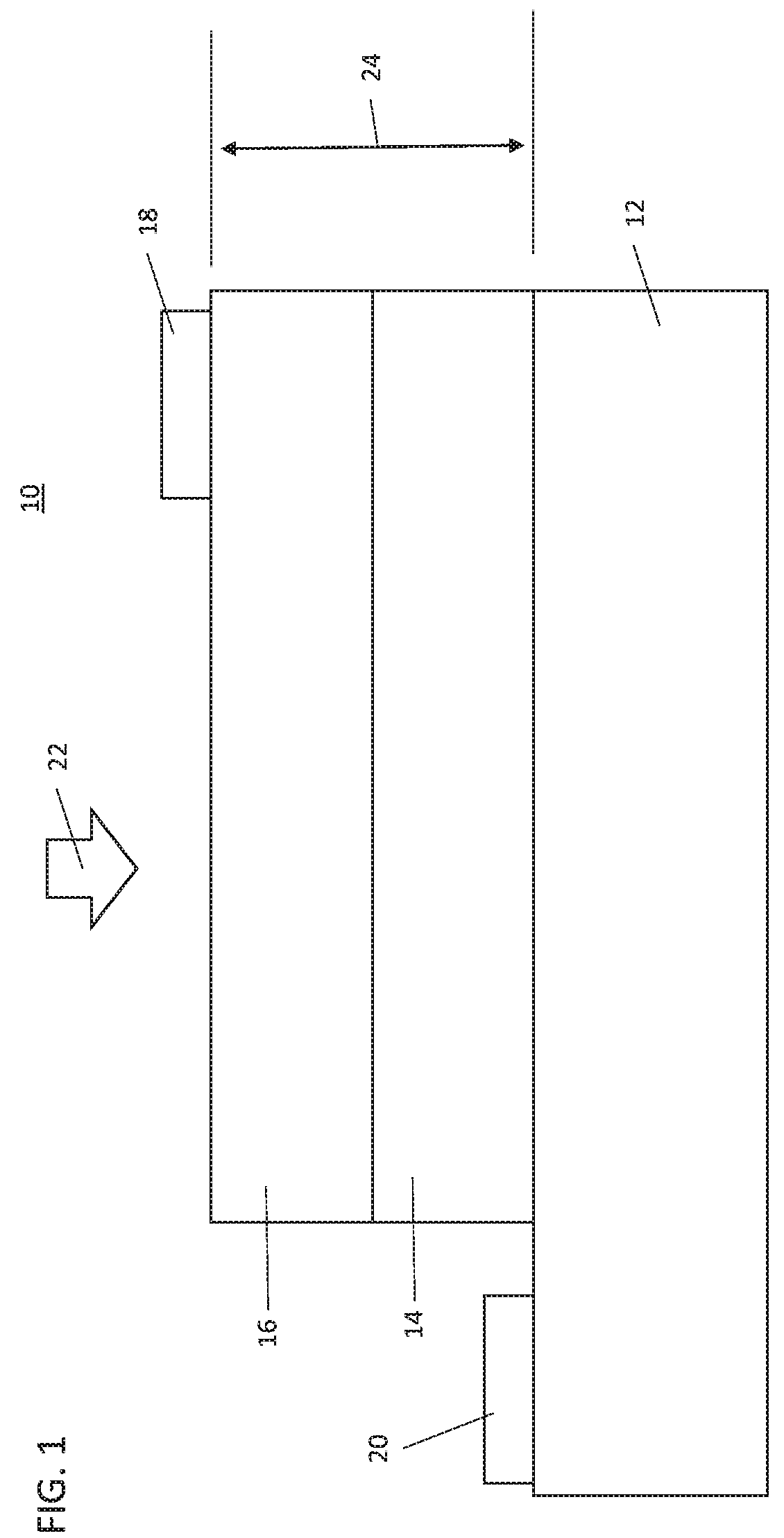
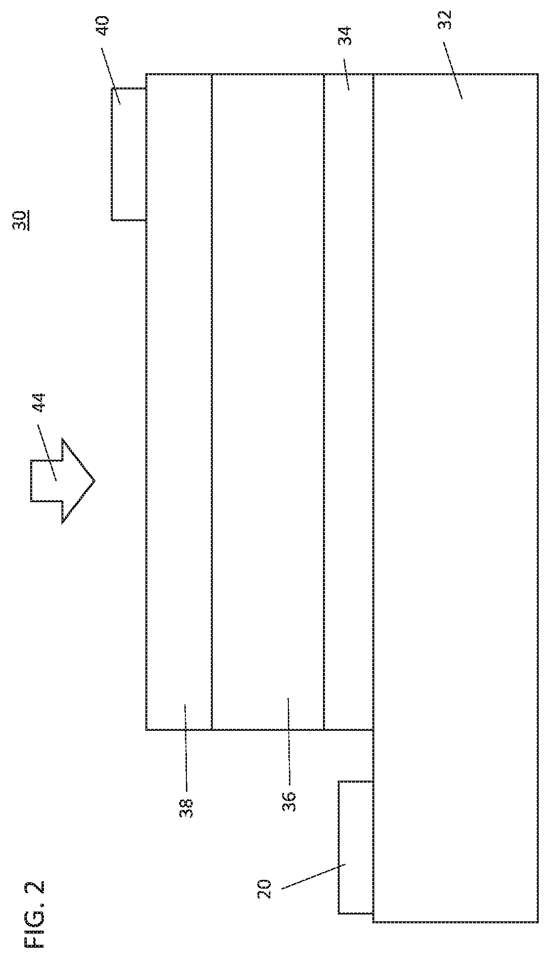
[0011]In accordance with embodiments of the present invention, photovoltaic devices are provided that employ wide bandgap semiconductor materials that are activated using short wavelength laser light or other portions of the electromagnetic spectrum to deliver high voltage using a single photovoltaic cell. While tandem cells may be employed, the single photovoltaic cell provides ease of manufacture and ease of incorporation into other devices and systems. In particularly useful embodiments, materials employed for the high voltage photovoltaic devices can include materials having bandgaps greater than about 2 eV. These high bandgap materials are considered inefficient for photovoltaic device use due at least to the high barrier energy to be overcome to cause conduction.

[0012]The high voltage photovoltaic devices can be made having small sizes, e.g., less than about 100 microns, to fit in or on electronic devices. The high voltage photovoltaic devices can provide output voltage ranges...


PUM


Abstract

A photovoltaic device includes a substrate and a P-type layer having a first electrode formed on a surface of the P-type layer. An N-type layer has a second electrode formed on a surface of the N-type layer. The P-type layer and the N-type are formed from a common base material. The base material includes a bandgap of at least 2 electron-volts such that a potential across the first and second electrodes is greater than 2 volts when the device is exposed to light.

Description

BACKGROUNDTechnical Field[0001]The present invention generally relates to photovoltaic devices, and more particularly to devices for generating high voltage for powering electronic devices including devices employed for Internet of things (IoT) applications.Description of the Related Art[0002]Remote power sources are needed for Internet of things (IoT) applications and other portable devices. Many devices in the IoT need sustained energy with a higher voltage requirement than currently available in photovoltaic devices. Conventional photovoltaic devices usually provide voltages of less than 1 volt to about less than about 1.8 volts. This is insufficient for many applications. Traditional high voltage solutions include attaching multiple cells laterally and connecting the cells in series or tandem cells. However, these solutions may not provide the voltage potentials needed to proficiently run many device operations.SUMMARY[0003]In accordance with an embodiment of the present inventi...

Claims


Application Information

Patent Timeline
IPC IPC(8): H01L31/075H01L31/068H01L31/028H01L31/0304H01L31/0352
CPCH01L31/075H01L31/068H01L31/035236H01L31/03044H01L31/0304H01L31/028H01L31/03048H01L31/0312Y02E10/544Y02E10/547Y02E10/548Y02P70/50
Inventor BEDELL, STEPHEN W.LI, NINGSADANA, DEVENDRA K.SHAHIDI, GHAVAM G.
Owner IBM CORP
Why Eureka
Try Eureka